鑫景福致力于滿足“快速服務,零缺陷,輔助研發”PCBA訂購單需求。


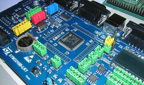
PCBA加工
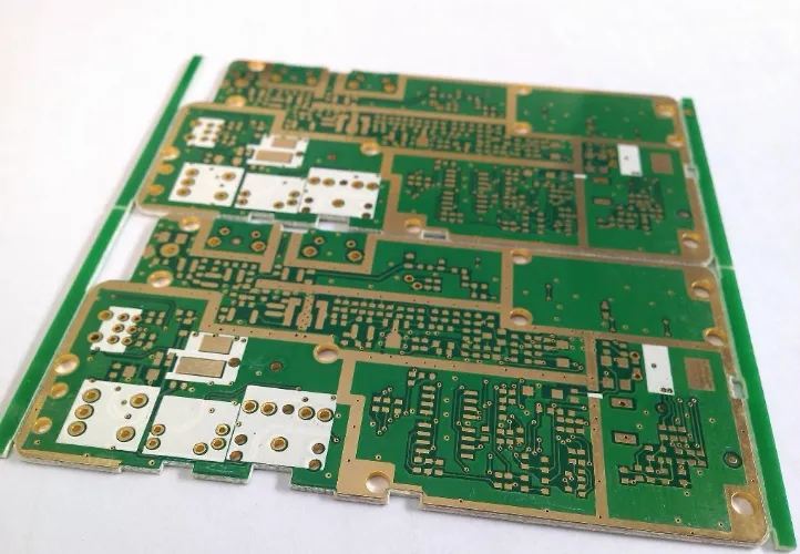
PCB process PCB (printed circuit board) processing and production process
The raw material of PCB (printed circuit board) is glass fiber, whICh can be seen everywhere in our daily life. For example, the core of fire-proof cloth and fire-proof felt is glass fiber. Glass fiber is easy to combine with resin. We immerse the glass fiber cloth with compact structure and high strength into the resin, and then harden it to obtain a PCB substrate with thermal insulation and resistance to bending. If the PCB board is broken, the edge is white and layered, It is sufficient to prove that the material is resin glass fiber.
It is impossible for us to transmit electrical signals with insulating boards alone, so we need to cover the surface with copper. So we also call PCB as copper clad substrate. In the factory, the common code of copper clad substrate is FR-4, which is not different among board and card manufacturers, so we can think that everyone is on the same running line. Of course, if it is high-frequency board, it is better to use the copper clad PTFE glass cloth laminate with higher cost.
The copper coating process is very SIMple. Generally, it can be made by calendering and electrolysis. The so-calLED calendering is to paste high-purity (>99.98%) copper onto the PCB substrate by rolling -- because the epoxy resin and copper foil have excellent adhesion, the copper foil has high adhesion strength and working temperature, and can be DIPped welded in 260 ℃ molten tin without blistering. This process is quite like rolling dumpling skin, the thinnest can be less than 1mil (industrial unit: mil, that is, one thousandth of an inch, equivalent to 0.0254mm). If the skin of the dumpling is so thin, it will leak in the pot! The so-called electrolytic copper has been learned in junior high school chEMIstry. CuSO4 electrolyte can continuously produce layers of "copper foil", which is easy to control the thickness. The thicker the copper foil is, the more time it takes! Generally, the factory has strict requirements on the thickness of copper foil, which is generally between 0.3mil and 3mil. A special copper foil thickness tester is used to check the quality. The PCB used by ancient radios and amateurs is particularly thick coated with copper, which is far inferior to the quality in the computer board factory.
The control of copper foil thickness is mainly based on two reasons: one is that uniform copper foil can have a very uniform resistance temperature coefficient and low dielectric constant, which can reduce the signal transmission loss. This is different from the capacitance requirement, which requires a high dielectric constant, so that it can accommodate higher capacity in a limited volume. Why is the resistance SMAller than the capacitance? In the final analysis, the dielectric constant is high! Secondly, the temperature rise of thin copper foil is small when passing large current, which is very beneficial to heat dissipation and component life. It is also the reason that the width of copper wire in digital integrated circuit should be less than 0.3cm. The well made PCB finished board is very uniform and has a soft luster (because the surface is brushed with solder resist), which can be seen by the naked eye, but few people can see the good or bad of the copper clad substrate, unless you are an experienced product inspector in the factory.
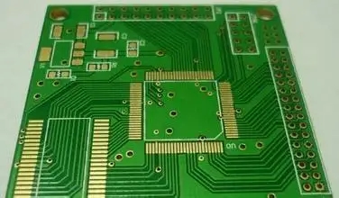
For a PCB substrate wrapped with copper foil, how can we place components on it to achieve signal conduction between components instead of the whole board? The twisted copper wires on the board are used to transmit electrical signals. Therefore, we only need to erode the unused parts of the copper foil and leave the copper wires. To achieve this step, first of all, we need to understand a concept, that is, "line negative" or "line film". We use a lithography machine to print the circuit design of the board into film, and then cover the substrate with a photosensitive dry film whose main components are sensitive to specific spectrum and react chemically. There are two types of dry films, photopolymerization type and photodegradation type. Photopolymerization type dry films will harden under the light of specific spectrum, From water-soluble substances to water-insoluble ones, the photo decomposing ones are just the opposite.
Here, we use photopolymerization type photosensitive dry film to cover the substrate first, and then cover it with a layer of line film to expose it. The exposed area is black and opaque, otherwise it is transparent (line part). Light shines on the photosensitive dry film through the film -- what's the result? The color of the dry film on the transparent part of the film becoMES darker and begins to harden. It tightly wraps the copper foil on the surface of the substrate, just like printing the circuit diagram on the substrate. Next, we go through the development step (use sodium carbonate solution to wash the unhardened dry film) to expose the copper foil that does not need dry film protection, which is called stripping process. Next, we use copper etching solution (chemicals that corrode copper) to etch the substrate. The copper without dry film protection is completely destroyed. The circuit diagram under the hardened dry film is shown on the substrate. The whole process is called "image transfer", which plays a very important role in PCB manufacturing. The next step is to make multilayer boards. According to the above steps, only a single panel is made, even if the two sides are only double-sided boards, but we can often find that the boards in our hands are 4-layer boards or 6-layer boards (even 8-layer boards).
With the above foundation, we understand that it is not difficult to make two double-sided boards "stick" together! For example, we make a typical four layer board (divided into 1~4 layers in order, of which 1/4 is the outer layer, signal layer, 2/3 is the inner layer, grounding layer and power supply layer). First, we make 1/2 and 3/4 (the same base plate) respectively, and then stick one of the two base plates. Is it OK? However, this adhesive is not an ordinary glue, but a resin material in a softened state. It is insulating first, thin second, and has good adhesion with the substrate. We call it PP material. Its specifications are thickness and resin content. Of course, we can't see the thickness of the four ply board and six ply board generally, because the thickness of the six ply board is relatively thin. Even if two layers of PP and three double-sided boards are used, we can't see how much more thick the four ply board with one layer of PP and two double-sided boards can increase -- the thickness of the board card has certain specifications, otherwise it can't be inserted into various card slots. At this point, the reader will ask, isn't the signal between the Multi layer boards to be connected? Now PP is an insulating material, how to realize the interconnection between layers? Don't worry, we need to drill holes before bonding the multilayer boards! If the holes are drilled, the corresponding copper wires at the upper and lower positions of the circuit board can be aligned, and then the hole wall is coated with copper. Isn't that equivalent to the wires connecting the circuits in series?
This kind of hole is called Plating hole (PT hole for short). These holes need to be drilled by a drilling machine. Modern drilling machines can drill very small holes and shallow holes. There are hundreds of holes of different sizes and depths on a motherboard. We use a high-speed drilling machine to drill them for more than an hour. After drilling, we can conduct hole electroplating (This technology is called Plated Through Hole Technology, PTH) to make the hole conductive. The holes have also been drilled, the inner and outer layers have been passed, and the Multilayer boards have been glued. Is it over? Our answer is "No", because motherboard production requires a lot of welding. If it is directly welded, there will be two serious consequences:
1、 The copper wire on the board surface is oxidized and cannot be soldered;
2、 Overlap welding is serious -- because the distance between wires is too small! Therefore, we must coat the entire PCB substrate with another layer of armor -- this is the solder mask, which is also known as solder mask. It has no affinity for liquid solder, and will change and harden under the light of specific spectrum. This feature is similar to the dry film. The color of the board we see is actually the color of the solder mask. If the solder mask is green, the board is green.
Finally, don't forget screen printing, gold finger plating (for graphics cards or PCI cards) and quality inspection. Test whether there is a short circuit or an open circuit in the PCB, using optical or electronic methods. Scanning is used optically to find out the defects of each layer, and flying probe is usually used for electronic testing to check all connections. Electronic testing is more accurate in finding short circuits or open circuits, but optical testing can more easily detect the problem of incorrect gaps between conductors.
To sum up, the production process of a typical Pcb factory is as follows:
Blanking → inner layer fabrication → pressing → drilling → copper plating → outer layer fabrication → anti welding paint printing → text printing → surface treatment → contour processing.
Purpose: According to the requirements of the engineering data MI, cut the large plates that meet the requirements into small pieces for production. Small plates that meet customer requirements
Process: large plate → plate cutting according to MI requirements → curium plate → fillet, edge grinding → plate out
Purpose: According to the engineering data (customer data), drill the required hole diameter at the corresponding position on the sheet with the required size. Process: laminated pin → upper plate → drilling → lower plate → inspection/repair
3、 Purpose of copper sinking: copper sinking is to deposit a thin layer of copper on the wall of insulating hole by chemical method. Process: rough grinding → hanging plate → automatic copper sinking line → lower plate → dipping 1% dilute H2SO4 → thickening copper
4、 Graphic transfer
Purpose: Graphic transfer refers to the process of transferring images on production film to the plate: (blue oil process): plate grinding → printing the first side → drying → printing the second side → drying → lighting → developing → inspection; (Dry film process): hemp board → pressing film → standing → alignment → exposure → standing → developing → inspection V. Pattern electroplating
Purpose: Pattern electroplating refers to electroplating a copper layer with the required thickness and a gold nickel or tin layer with the required thickness on the exposed copper skin or hole wall of the circuit pattern
Process: upper plate → degreasing → secondary water washing → micro etching → water washing → acid washing → copper plating → water washing → pickling → tin plating → water washing → lower plate Purpose: use NaOH solution to remove the anti electroplating coating to expose the non circuit copper layer
Process: water film: rack inserting → alkali dipping → flushing → scrubbing → machine passing; Dry film: plate placing → machine passing
7、 Etching purpose: Etching is to use chemical reaction method to erode the copper layer of non circuit parts
8、 Purpose of green oil: green oil is to transfer the pattern of green oil film to the plate, which plays the role of protecting the circuit and preventing the tin on the circuit when welding parts. Process: plate grinding → printing light sensitive green oil → corner plate → exposure → development; Grinding plate → printing the first side → drying plate → printing the second side → drying plate Purpose
9、 Gold plated finger Purpose: to coat the plug finger with a nickel/gold layer of required thickness to make it more hard and wear-resistant Process: upper plate → degreasing → twice washing → micro etching → twice washing → pickling → copper plating → water washing → nickel plating → water washing → gold plating
10、 Purpose of tin plating plate: tin spraying is to spray a layer of lead tin on the bare copper surface not covered with solder resist oil to protect the copper surface from corrosion and oxidation, so as to ensure good welding performance. Process: micro etching → air drying → preheating → rosin coating → solder coating → hot air leveling → air cooling → washing and air drying
11、 Molding purpose: the method of forming the shape required by customers through die stamping or numerical control gongs and machines. Organic gongs, beer boards, hand gongs, and hand cutting. Note: The accuracy of data gongs and beer boards is high, followed by hand gongs. Hand cutting boards can only make some simple shapes
12、 Test purpose: through electronic 100% test, detect open circuit, short circuit and other defects affecting functionality that are not easily found by visual inspection.


抖音二維碼

Q Q二維碼

微信二維碼
點擊
然后
聯系
然后
聯系
電話熱線
13410863085Q Q

微信

- 郵箱