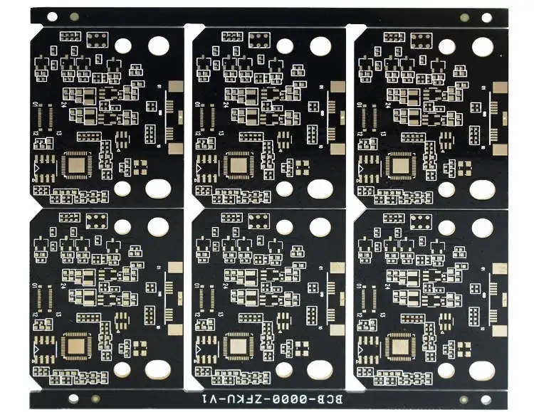
鑫景福致力于滿足“快速服務(wù),零缺陷,輔助研發(fā)”PCBA訂購單需求。


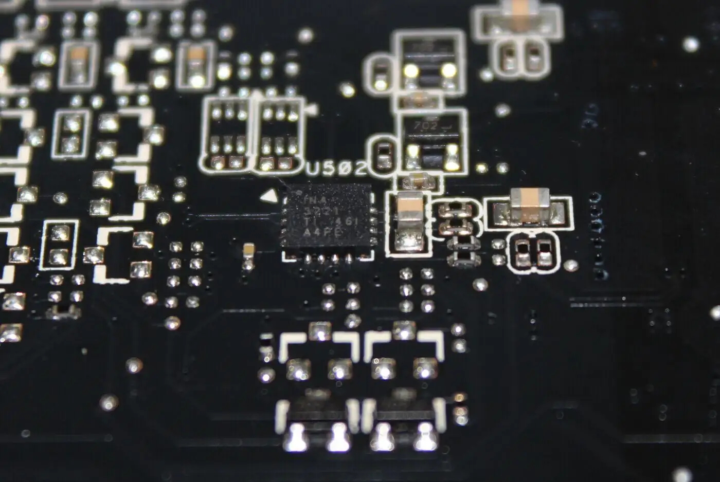
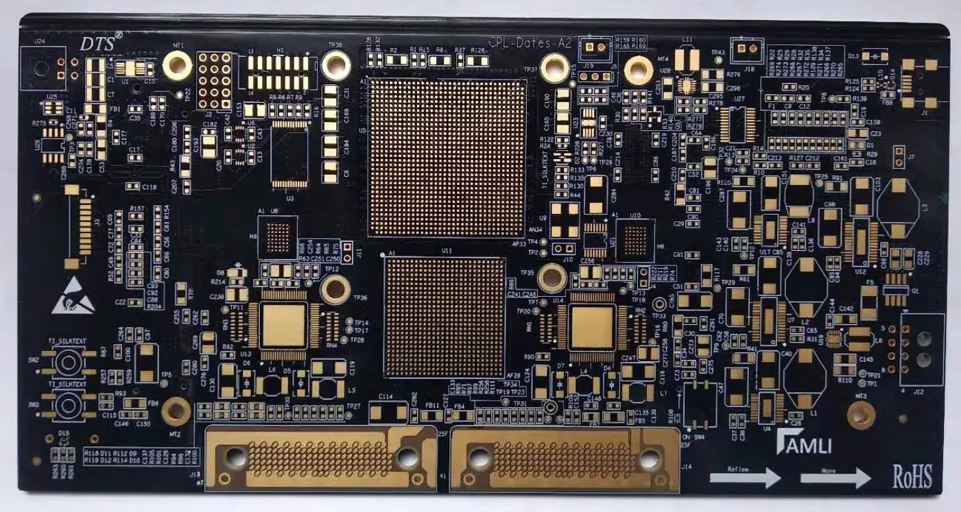
PCBA加工
PCBA assembly precautions and Production requirements
Due to the increasingly thin and thin shape and line width of the IC, the IC is vulnerable to damage by EOS and ESD, resulting in permanent failure. Analysis shows that the defects caused by EOS and ESD occupy the top three. Although necessary measures are taken in the design to ensure the reliability of the IC, the damage to the IC caused by EOS and ESD cannot be effectively eliminated. It is also necessary to control the production process to avoid destructive damage to the IC caused by EOS and ESD. At the same time, the storage and use of IC do not meet the requirements, which often leads to "popcorn" and "delamination" during SMT processing, which is also an important reason for IC damage. Here we discuss how to avoid damaging IC in the PCBA manufacturing process and promote the improvement of production quality.
Packaging and storage of IC:
If the IC is exposed to the air for a long time, it will absorb moisture in the air, which will lead to the so-calLED "popcorn" phenomenon in the SMT process, resulting in IC failure. Therefore, the IC must be baked before packaging or use. IC is baked at 125 ℃ for 7 hours before ACTIONS leaves the factory, and then vacuum packed to ensure that IC can be stored for 12 months at 40 ℃ and relative humidity below 90%. If IC is in this environmental time, customer can perform SMT welding procedure within 72 hours after unpacking (environmental requirements: 30 ℃ and relative humidity below 60%), otherwise IC must be baked again. If the IC is not used up within 72 hours, it must be baked to remove the IC moisture absorption problem. Baking condition: bake at 125 ± 5 ℃ for at least 12 hours. After baking, add appropriate amount of desiccant for vacuum packaging or arrange SMT welding production in time within 4 hours.
Factory environmental control recommendations: 18-25 ℃, 40-60% relative humidity. Meaning of humidity indicator card: the displayed value should be less than 5% (blue). If it is greater than 5% (pink), it means that the IC has absorbed moisture.
Inventory control principle: first in, first out. The label on the vacuum packaging bag explains to the moisture sensitive device: the customer is requested to list the above precautions for IC storage and use control into the internal warehouse management, SMT process operation control and other operation specifications and implement them.
POP CORN phenomenon:
When the molded package or IC is exposed in a humid and hot environment, when there is water between the chip and the resin, wiring and resin, or the resin contains hydroxyl, which is easy to absorb moisture. When the water absorption rate increases, the water will immediately vaporize and expand, and the resin will also expand, causing cracks in the IC body or pulling the wiring in the IC. Therefore, attention should be paid to the environmental requirements in IC packaging and storage to avoid IC damage due to environmental factors. ESD and EOS protection measures in the process
ESO: Type of IC failure caused by EOS:
1. System transient pulse (STP)
2. Lightning
3. Electrostatic discharge (ESD)
4. Electromagnetic pulse (EMP)
All of these may lead to the melting of metal compounds or bonding wires and the failure of IC. Causes of EOS in production
1. Incorrect working procedure: for example, there is no standard operating procedure, the component polarity is misplaced, the IC is taken when starting up, and the system is powered on before the installation is completed;
2. No EOS control equipment, especially in noisy environment;
3. Incorrectly test components, such as fast transfer switch, improper voltage setting, etc;
4. Poor power supply;
5. There is no proper equipment maintenance and power supply monitoring: such as intermittent accidents caused by loose contacts, ungrounded equipment, etc.
EOS prevention:
1. Establish appropriate operation procedures;
2. Ensure proper IC testing;
3. Good power supply;
4. Maintain strict equipment/fixture/adapter card maintenance system
ESD: Electrostatic discharge
Causes of ESD:
1. Human body; 2. Equipment and machinery; 3. Loading process. ESD prevention: the source of reducing static voltage
2. The staff shall wear anti-static wrist strap, conductive clothes and shoes;
3. Anti static or conductive direct or indirect materials are widely used;
4. Establish safe electrostatic workstation and area;
5. Ensure that the equipment will not generate static electricity above 200V;
6. The relative humidity of the factory environment is maintained at 40-60%;
7. Use an air separator to attenuate the static voltage below 35V;
Precautions during SMT assembly:
1. The pin size and allowable error setting input of each IC component are correct.
2. Solder paste characteristics inspection and management
a. Inspection items: FLUX component content, particle size and viscosity inspection;
b. Solder paste management: The solder paste must be refrigerated at 2-8 ℃. It is best to print solder paste at 20-25 ℃ with a relative humidity of 40-50% RH. It is not allowed to directly blow cold or hot air. The performance of solder paste will be affected when the temperature exceeds 26.6 ℃. The storage time of the inventory shall not exceed three months, and the solder paste must be stirred for 2-3 minutes before use.
c. Preparation before using solder paste: temperature return. Do not open the container or stir the solder paste until the solder paste has returned to room temperature. Generally, the temperature recovery time is about 4-8 hours (natural temperature recovery). If the container is opened without temperature recovery, the solder paste will condense the moisture in the air, causing problems such as SLUMP and SPUTTER.
d. Solder paste should not be used for more than 8 hours. Solder paste recycled overnight should not be used.
3,SOLDER ALLOY CHART
4. PCB management
a. The warpage shall be strictly checked (avoid empty welding), and the warpage specification shall not be greater than 0.7% of the diagonal
b. The water absorption of PCB shall be less than 0.1%.
c. PCB baking: baking at 120 ℃ for 2 hours.
d. QFP/BGA IC shall not be designed on the diagonal of PCB as much as possible.
5. Description of REFLOW over welding temperature control
a. Preheat and Soak
Function: avoid rapid softening of the flux in the solder paste; Completely volatilize the volatiles in the flux; Mitigate the thermal shock during formal heating; It can promote the activation of flux and clean oxides and pollutants on PAD.
Effect: If the preheating is insufficient, the temperature difference between it and the formal heating is too large, which is easy to cause the solder ball nearby due to flow movement; If the pre baking is excessive, it will cause the aging of flux components and the oxidation of tin powder; If the temperature in the heating zone of molten tin rises rapidly, the temperature distribution will be uneven, leading to the so-called tombstone and wick effect.
b. Reflow soldering area:
Effect: If the heating temperature is insufficient, it is easy to cause cavities or cold welding; If the Peak temp temperature is too high or it is pulled too long above 183 ℃, the melted solder will be oxidized, resulting in defects such as reduced bonding degree.
c. Cooling area
Effect: If the cooling time is too fast, the substrate will be bent, resulting in reduced joint; If the cooling time is too slow, the welding structure will be coarsened.
6. Reflow soldering temperature curve and control
a. Temperature curve: it shall be considered according to the PC board size and component density of various products.
b. Control: regularly measure the temperature and continuously review the defective rate of solder joints; The temperature shall be controlled below 220 ℃.
7. Requirements and control of steel plate
a. Requirements: Generally, the opening of IC steel plate should be 10 microns SMAller than that of IC PAD, which can prevent solder paste from deviating 0.2 mm from the tin pad (PAD) to form solder balls; Without Undercut, it will prevent the solder paste from moving forward during printing; The hole wall is smooth and the front, middle and rear dimensions are the same
b. Control: check the thickness of printing solder paste every two hours; Every shift shall clean and maintain the steel plate before use every day to prevent blocking, pollution, deformation and other problems of the steel plate hole; The service life of the steel plate is generally about 80,000-100,000 printed substrates; Check the steel plate once after 10 tiMES of printing.
c. Process parameters of steel plate printing: scraper pressure, printing speed, printing gap/angle, good solder paste quality, environmental requirements: temperature: 18-25 ℃, humidity: 40-60% RH, adjusted according to different ICs and plates.
PCB inspection and test:
1. AOI: Automated Optical Inspection
2. AOI shall be used for SMT inspection
Missing parts: not affected by the substrate style
Offset: not affected by substrate style
Polar inversion: components with polarity symbols
Tombstone effect, wrong parts, less tin, tin bridge, empty soldering, excessive soldering
3. ICT (IN CIRCUIT TEST) equipment is used for PCBA test. During ICT test, attention should be paid to the defects caused by FLUX residues. Generally, in the PCBA test, AOI method shall be used to conduct appearance inspection first to check whether there are any defects listed in the previous page. After there is no abnormality, ICT shall be used to conduct device parameter/PCB OS test for PCBA. When there is no abnormality in these two tests, power on can be used for functional test. Precautions for Rework: For products that need to be reworked, in order to avoid "popcorn" and "delamination" in the IC when taking the IC,
The following steps must be followed during rework:
1. PCB must be baked to remove the moisture absorption of IC components. Baking requirements: bake at 100 ℃ for at least 12 hours;
2. After baking, when using the thermal blowing gun to take IC, the operation shall be carried out in strict accordance with the operating instructions of the thermal blowing gun, mainly including the temperature setting, the distance between the tuyere and IC, and the wind strength.
3. After baking, rework and new board operation shall be completed within 4 hours.
4. The IC storage and use after rework are consistent with those of normal products.


抖音二維碼

Q Q二維碼

微信二維碼
點擊
然后
聯(lián)系
然后
聯(lián)系
電話熱線
13410863085Q Q

微信

- 郵箱