鑫景福致力于滿足“快速服務,零缺陷,輔助研發”PCBA訂購單需求。


PCBA加工
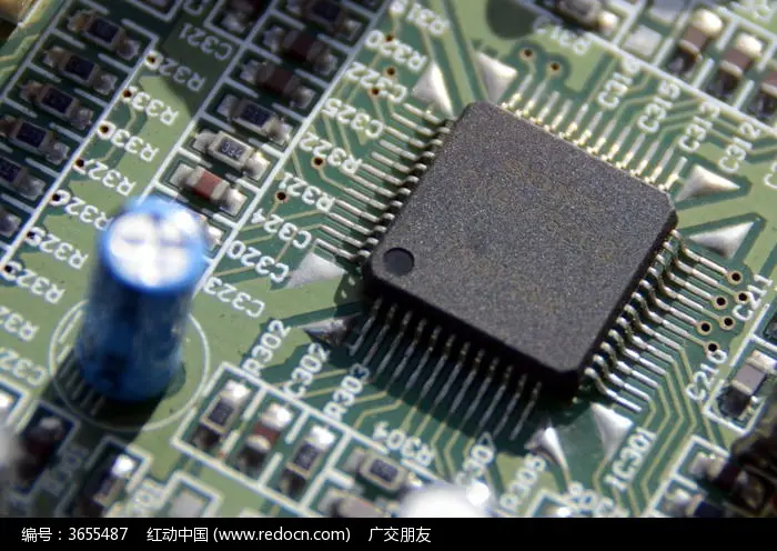
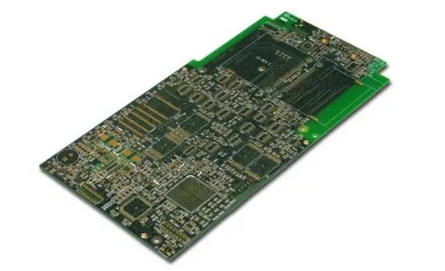
With the development of PCBA assembly of electronIC products towards miniaturization and high assembly density, SMT Surface Mount Technology has now become the mainstream technology of electronic assembly. However, due to the large size of some electronIC components in the assembly and processing of PCBA, plug-in processing has not been replaced, and still plays an important role in the electronic assembly and processing process, so there will be a certain number of through-hole plug-in components in the pcb circuit board. The assembly of both cartridge components and surface assembly components is calLED hybrid assembly, referred to as mixed assembly, and the assembly using all surface assembly components is called full surface mount. PCBA assembly method and process flow mainly depend on the type of components assembled and the equipment conditions assembled. What steps are involved in PCB assembly?

Step 1: Application of solder paste
This is the first step in PCB assembly. Before adding the components, you need to add the solder paste. Ming Hua Hang electric automatic printing machine. Solder paste needs to be added to the area of the circuit board where solder is to be applied. Apply solder paste to circuit board with the help of solder screen. It is placed in the correct position on the board, and the runner moves over it. This allows the solder paste to be squeezed through the hole and applied to the circuit board.
Step 2: Place the components
This is done after applying the solder paste. Surface mount technology (SMT) requires precise placement of components, which is difficult to achieve by manual placement. Therefore, the components are placed on the board with the help of a pick - up machine. The PCB design information provides information on where the components need to be placed and the components needed to pick up and place the machine. This SIMplifies the pick - up programming and makes it more accurate.
Step 3: Reflux furnace
In this step, the actual connection takes place. After placing the components, place the circuit board on the reflux furnace conveyor belt. The solder applied during welding melts during reflow. This permanently connects the component to the board.
Step 4: Wave crest welding
In this step, the PCB is placed on the system driven by the mechanical conveyor and passed through different areas. The PCB passes through a melt weld wave, which helps connect the PCB pads/holes, electronic component leads, and solder. This helps form electrical connections. It should be noted that different selective crest welding processes can be selected according to the number of components on the bottom surface. With different processes, the spacing and orientation requirements of components are also different. You can refer to the layout requirements of board components.
Step 5: Clean the PCB
It is very important to clean PCB after assembly. This process helps clean all flux residues with the help of ionized water.
Step 6: Check the PCB components
This is one of the most important steps in PCB assembly. Techniques such as X-rays and AOI are used to determine the quality of assembled PCBS. In this step, check the circuit board for short circuits, loose balls, and Bridges between balls.
Step 7: Test the board and monitor the output
This is the last step in the process. This step involves monitoring whether the product provides the desired output. The board is tested and analyzed for faults in several ways.
In soldering process, the SMAllest variables should belong to the machine equipment, so the first to check them, in order to achieve the correctness of the check, can be assisted by an independent electronic analyzer, such as thermometer detection of various temperatures, accurate calibration of machine parameters with an electric meter.
Short video community for electronics engineers
More than 5 million engineers are using it
Open the APP
Lee smile to
5-year user 151 experience points
Personal attention
Inspection of assembled printed circuit boards
To meet the requirements of PCB testing, a variety of testing equipment has been produced. Automatic optical inspection (AOI) system is usually used to test the inner layer before the formation of layers. After layering, the X-ray system monitors alignment accuracy and minor defects; The scanning laser system provides a method for detecting the pad layer prior to reflux. These systems, together with visual inspection technology on the production line and component integrity testing with automatically placed components, help ensure the reliability of the final assembly and welded plates.
However, even if these efforts minimize defects, there is still a need for final inspection of the assembLED PCB, which is perhaps the most important because it is the final unit of product and process evaluation.
The final inspection of the assembled printed circuit board may be done either by an active method or by an automated system, and often both methods are used. "Manual" means that an operator uses an optical instrument to visually inspect the board and make a correct judgment about defects. Automated systems use computer-aided graphic analysis to determine defects, and many people also believe that automated systems contain all detection methods except manual light detection.

X-ray techniques provide a method for estimating solder thickness, distribution, internal voids, cracks, dessoldering and the presence of solder spheres (MARKstein, 1993). Sonography will detect holes, cracks, and unglued joints. Automatic optical detection * Estimation of external features, such as bridging, tin melt and shape. Laser detection can provide three-dimensional images of external features. Infrared detection detects internal weld faults by comparing the thermal signal of the weld with that of a known good weld.
It is worth noting that these automatic detection techniques have been found for all defects that the limited detection of assembled printed circuit boards cannot detect. Therefore, the manual visual detection method must be used in conjunction with the automatic detection method, especially for those few applications. The combination of X-ray detection and manual optical detection is the best method to detect defects of assembly plates.
Note: in any case, try not to adjust the machine to overcome some temporary solder problems, such adjustments may lead to bigger problems! It should be from the actual work and records, to find the most appropriate operating conditions.
The most detailed SMT chip processing flow
11-05,2022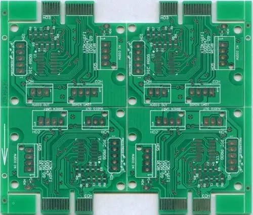


抖音二維碼

Q Q二維碼

微信二維碼
點擊
然后
聯系
然后
聯系
電話熱線
13410863085Q Q

微信

- 郵箱