鑫景福致力于滿足“快速服務,零缺陷,輔助研發”PCBA訂購單需求。


PCBA加工
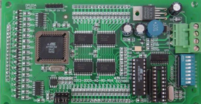
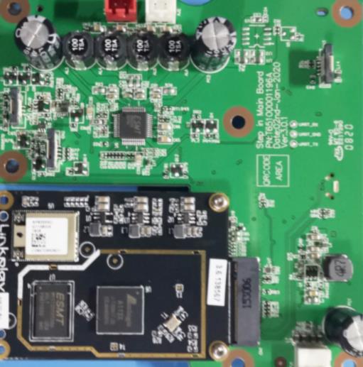
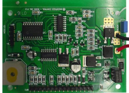
design using SMT components and PCBA circuit boards
Environmental conditions for storage SMT components:
Ambient temperature: inventory temperature<40 ℃.
The temperature at the production site is lower than 3.0 ℃.
Ambient humidity:
Ambient air: sulfur, chlorine, acid and other toxIC gases that affect welding efficiency shall not exist in the storage and use environment.
Anti static measures: meet the anti-static requirements of SMT components.
Storage period of components: calculated from the production date of the component manufacturer, the storage time shall not exceed 2 years; The inventory time of the complete machine factory users after purchase generally does not exceed one year; If it is a complete machine factory with relatively humid natural environment, the purchased SMD components should be used within 3 months after import, and appropriate moisture-proof measures should be taken on the storage location and component packaging.
SMD equipment with moisture resistance requirements. It must be used up within 72 hours after opening, and no longer than one week. If it cannot be used up, it should be stored in a RH20% drying box. The wet patch equipment shall be dried and dehumidified as required.
There are two types of plastic pallets for QFP packaging: non high temperature resistant and high temperature resistant. High temperature resistance (Tmax=135 ° C, 150 ° C or max180 ° C, etc.) can be directly put into the oven for baking; Those that are not resistant to high temperature cannot be directly put into the oven for baking. In order to prevent accidents, they should be separately placed in a metal pan for baking. Avoid damaging the pin during transfer to avoid damaging its coplanarity.
SMT components
Transportation, data separation, inspection or manual placement:
If workers need to use SMD equipment, they should wear an anti-static wrist strap, use an oil suction pen as much as possible, and pay special attention to avoid bumping the pins of SOP, QFP and other equipment to prevent the pins from warping.
Use original and complete packaging bags. As long as the bag is not damaged and the desiccant inside is in good condition (all black circles on the humidity instruction card are blue, no pink), unused SMDs can still be repackaged into the bag and seaLED with adhesive tape.
Precautions in Design PCBA circuit board
circuit design
1. For standard components, attention should be paid to the dimensional tolerance of components from different manufacturers. For non-standard components, the pad pattern and pad spacing must be designed according to the actual size of the component.
2. When designing a circuit with high reliability, the pad shall be widened, and the pad width=1.1~1.2 tiMES the width of the component welding end.
3. In the design of high-density PCBA, the pad size of components in the software library should be corrected
4. The distance between various components, wires, test points, through holes, pads and wiring, solder mask, etc. must be designed according to different processes.
5. Consider repairability.
6. Consider heat dissipation, high frequency and anti electromagnetic interference.
7. The position and direction of elements shall be designed according to the requirements of reflow or wave soldering process. For example, when using the reflow soldering process, the placement direction of components should consider the direction of PCB entering the reflow soldering furnace. When used; When wave soldering, PLCC, FP, connector and large size SOIC components cannot be placed on the wave soldering surface; In order to reduce the wave shadow effect and improve the welding quality, there are special requirements for the placement direction and position of various components; When designing wave crest pad pattern, the pad length of rectangular element, SOT and SOP element shall be extended, and the two pairs of SOP pads at the outermost layer shall be widened to absorb excess solder, and both ends of the pad can be chamfered at 45 ° to less than 3.2mm × 1.6mm rectangular element, and so on.
8. Equipment shall also be considered in PCB design. Different mounters have different mechanical structures, alignment methods and PCB transmission methods. In this case, the position of the positioning hole of the PCB, the figure and position of the reference MARK (mark), the edge shape of the PCB and the PCB are different. There are different requirements for components that cannot be placed near the side of the circuit board. If the wave soldering process is used, the process margin that needs to be left in the transmission chain of the printed circuit board should also be considered.


抖音二維碼

Q Q二維碼

微信二維碼
點擊
然后
聯系
然后
聯系
電話熱線
13410863085Q Q

微信

- 郵箱