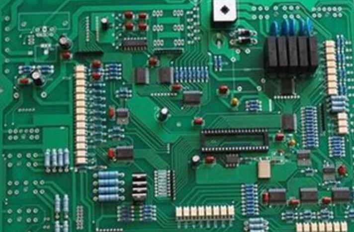
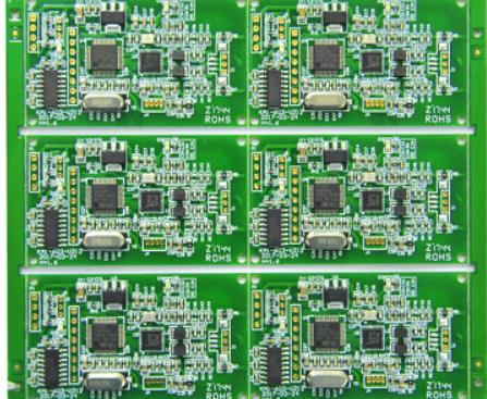
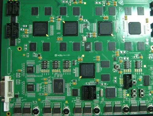
鑫景福致力于滿足“快速服務,零缺陷,輔助研發(fā)”PCBA訂購單需求。


PCBA加工
SMT needs to conduct incoming inspection and equipment cracking
SMT patch processing for incoming inspection required before
The inspection before SMT wafer processing is the primary condition to ensure the wafer quality. The quality of components, printed circuit boards and SMT chips directly affects the quality of PCB. In this regard, strICt incoming inspection and management system must be established for the electrical performance parameters of components, solderability of solders and pins, productivity design of printed circuit boards, and solderability of SMT patch materials such as pads, solder pastes, pastes, solder rods, fluxes, and cleaning agents. The quality problems of components, printed circuit boards and smt chip materials are difficult to solve in the subsequent process.
Let's introduce what inspection work should be done before processing.
1 Check SMT components:
The main inspection items of components include solderability, pin coplanarity and usability, which shall be sampLED by the inspection department. In order to test the solderability of the component, the stainless steel tweezers can fix the component body and immerse it in a tin pot at 235. ± 5 ℃ or 230 ± 5 ℃, and then take it out at a temperature of 2 ± 0.2s or 3 ± 0.5s. Check the welding end of the solder under a 20x microscope, and the welding amount of the welding end of the component is required to exceed 90%.
1. Visually or with a magnifying glass, check the welding end or pin surface of the assembly for oxidation or contamination.
2. The nominal value, specification, model, accuracy and overall dimension of parts shall meet the product process requirements.
3. The SOT and SOIC pins are not deformed. For multi lead QFP devices with lead spacing less than 0.65mm, the pin coplanarity should be less than 0.1mm (optical inspection through the mounter).
4. For the products to be cleaned, the MARKs of the parts after cleaning will not fall off, nor will they affect the efficiency and reliability of the parts (visual inspection after cleaning).
2. PCB inspection
(1) PCB grounding pattern and size, welding mask, screen and through-hole settings shall meet the design requirements of SMT printed circuit board. (For example, check whether the pad spacing is reasonable, whether the screen is printed on the pad, whether vias are made on the pad, etc.).
(2) The external dimensions of PCB shall be consistent, and the external dimensions, positioning holes and reference marks of PCB shall meet the requirements of production line equipment.
(3) Allowable warping size of PCB:
1. Upper/convex face: the maximum length is 0.2mm/50mm, and the maximum length is 0.5mm/the length direction of the entire PCB.
2. Down/concave: maximum 0.2mm/50mm length, maximum 1.5mm/length direction of the whole PCB.
(4) Check the PCB for contamination or moisture
As for the quality of SMT patch data, I believe that most patch processing plants will have no problems. The above is the check before patch processing. I hope friends in the electronics industry can learn more.
Solution for cracking SMT chip processing equipment
For MLCC capacitor, its structure is composed of laminated ceramic capacitor. In this case, its structure is weak, its strength is low, and it has strong heat resistance and mechanical impact, which is particularly obvious in wave soldering.
2. During SMT placement, the suction and release height of the Z-axis of the placement machine, especially for some placement machines that do not have the Z-axis soft landing function, depends on the thickness of the chip assembly, not through the pressure sensor. The tolerance of the thickness of this assembly may cause cracks.
3. After welding, if there is warping stress on PCB, it is easy to cause component cracking.
4. PCB stresses during splicing can also damage components.
Mechanical stress during ICT testing resulted in equipment breakage.
Stress during assembly can damage the MLCC around the fastening screws.
Solution to SMT chip processing equipment
1. Carefully adjust the welding process curve, especially the heating speed should not be too fast.
2. During placement, please ensure that the machine pressure is correctly placed, especially for thick plates and metal substrates, as well as ceramic substrates used to install MLCC and other brittle equipment
3. Pay attention to the placement method and shape of the tool.
4. The warpage of PCB, especially after welding, shall be specially corrected to prevent the stress caused by large deformation from affecting the device.
5. During this period, PCB is designed to avoid high stress areas of MLCC and other equipment
SMT patch processing for incoming inspection required before
The inspection before SMT wafer processing is the primary condition to ensure the wafer quality. The quality of components, printed circuit boards and SMT chips directly affects the quality of PCB. In this regard, strICt incoming inspection and management system must be established for the electrical performance parameters of components, solderability of solders and pins, productivity design of printed circuit boards, and solderability of SMT patch materials such as pads, solder pastes, pastes, solder rods, fluxes, and cleaning agents. The quality problems of components, printed circuit boards and smt chip materials are difficult to solve in the subsequent process.
Let's introduce what inspection work should be done before processing.
1 Check SMT components:
The main inspection items of components include solderability, pin coplanarity and usability, which shall be sampLED by the inspection department. In order to test the solderability of the component, the stainless steel tweezers can fix the component body and immerse it in a tin pot at 235. ± 5 ℃ or 230 ± 5 ℃, and then take it out at a temperature of 2 ± 0.2s or 3 ± 0.5s. Check the welding end of the solder under a 20x microscope, and the welding amount of the welding end of the component is required to exceed 90%.

1. Visually or with a magnifying glass, check the welding end or pin surface of the assembly for oxidation or contamination.
2. The nominal value, specification, model, accuracy and overall dimension of parts shall meet the product process requirements.
3. The SOT and SOIC pins are not deformed. For multi lead QFP devices with lead spacing less than 0.65mm, the pin coplanarity should be less than 0.1mm (optical inspection through the mounter).
4. For the products to be cleaned, the MARKs of the parts after cleaning will not fall off, nor will they affect the efficiency and reliability of the parts (visual inspection after cleaning).
2. PCB inspection
(1) PCB grounding pattern and size, welding mask, screen and through-hole settings shall meet the design requirements of SMT printed circuit board. (For example, check whether the pad spacing is reasonable, whether the screen is printed on the pad, whether vias are made on the pad, etc.).
(2) The external dimensions of PCB shall be consistent, and the external dimensions, positioning holes and reference marks of PCB shall meet the requirements of production line equipment.
(3) Allowable warping size of PCB:
1. Upper/convex face: the maximum length is 0.2mm/50mm, and the maximum length is 0.5mm/the length direction of the entire PCB.
2. Down/concave: maximum 0.2mm/50mm length, maximum 1.5mm/length direction of the whole PCB.
(4) Check the PCB for contamination or moisture
As for the quality of SMT patch data, I believe that most patch processing plants will have no problems. The above is the check before patch processing. I hope friends in the electronics industry can learn more.
Solution for cracking SMT chip processing equipment
For MLCC capacitor, its structure is composed of laminated ceramic capacitor. In this case, its structure is weak, its strength is low, and it has strong heat resistance and mechanical impact, which is particularly obvious in wave soldering.
2. During SMT placement, the suction and release height of the Z-axis of the placement machine, especially for some placement machines that do not have the Z-axis soft landing function, depends on the thickness of the chip assembly, not through the pressure sensor. The tolerance of the thickness of this assembly may cause cracks.
3. After welding, if there is warping stress on PCB, it is easy to cause component cracking.
4. PCB stresses during splicing can also damage components.
Mechanical stress during ICT testing resulted in equipment breakage.
Stress during assembly can damage the MLCC around the fastening screws.
Solution to SMT chip processing equipment
1. Carefully adjust the welding process curve, especially the heating speed should not be too fast.
2. During placement, please ensure that the machine pressure is correctly placed, especially for thick plates and metal substrates, as well as ceramic substrates used to install MLCC and other brittle equipment
3. Pay attention to the placement method and shape of the tool.
4. The warpage of PCB, especially after welding, shall be specially corrected to prevent the stress caused by large deformation from affecting the device.
5. During this period, PCB is designed to avoid high stress areas of MLCC and other equipment


抖音二維碼

Q Q二維碼

微信二維碼
點擊
然后
聯(lián)系
然后
聯(lián)系
電話熱線
13410863085Q Q

微信

- 郵箱