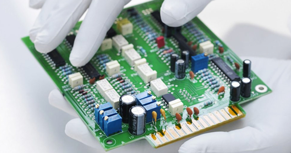
鑫景福致力于滿足“快速服務,零缺陷,輔助研發”PCBA訂購單需求。


PCBA加工
Six Keys to Chip Manufacturing
Shenzhen PCB manufacturer explains the six key steps of chip manufacturing that PCBA engineers must know
In the process of updating and iteration of many digital products, such as SMArt phones, technologICal changes have occurred quietly. Apple A15 bionIC chip and other cutting-edge chips are making more innovative technologies possible. How are these chips manufactured, and what are the key steps?
The powerful performance of modern digital products such as smart phones, personal computers and game consoles need no more words, and most of these powerful performance coMES from those very small but complex technological products - chips. The world has been surrounded by chips: in 2020, the world produced more than one trillion chips, which is equivalent to 130 chips owned and used by each person on the earth. However, even so, the recent chip shortage still shows that this number has not reached the upper limit.
Although chips can be produced on such a large scale, it is not easy to produce chips. The process of Chip Manufacturing is very complex. Today, we will introduce the six most critical steps: deposition, photoresist coating, lithography, etching, ion implantation and packaging.
deposition
The deposition step starts from the wafer, which is cut from 99.99% pure silicon cylinder (also calLED "silicon ingot") and polished to be extremely smooth, and then the conductor, insulator or semiconductor material film is deposited on the wafer according to the structural requirements, so that the first layer can be printed on it. This important step is often referred to as "deposition".
As chips become smaller and smaller, printing patterns on wafers becomes more complex. The progress of deposition, etching and lithography technology is the key to keep the chip smaller and smaller, thus promoting the continuity of Moore's Law. This includes innovative technologies that use new materials to make the deposition process more accurate.
Photoresist coating
The wafer is then coated with a photosensitive material called "photoresist" (also called "photoresist"). There are also two kinds of photoresists - "positive photoresist" and "negative photoresist".
The main difference between positive and negative photoresists lies in the chEMIcal structure of the material and the way photoresists react to light. For positive photoresist, the area exposed to ultraviolet light will change its structure and become more soluble, thus preparing for etching and deposition. Negative photoresist, on the contrary, will polymerize in the area exposed to light, which will make it more difficult to dissolve. Positive photoresist is used most in semiconductor manufacturing, because it can achieve higher resolution, which makes it a better choice for lithography stage. Nowadays, many companies in the world produce photoresists for semiconductor manufacturing.
Photolithography
Lithography is very important in the process of chip manufacturing, because it determines how small the transistors on the chip can be. At this stage, the wafer will be put into the lithography machine (yes, the product produced by ASML) and exposed to deep ultraviolet light (DUV). Many times their fineness is thousands of times smaller than that of sand grains.
The light will be projected onto the wafer through the "mask". The optical system of the lithography machine (the lens of the DUV system) will reduce the circuit pattern designed on the mask and focus on the photoresist on the wafer. As previously described, when light shines on the photoresist, chemical changes will occur to print the pattern on the mask onto the photoresist coating.
Making the exposed pattern completely correct is a tricky task. Particle interference, refraction and other physical or chemical defects may occur in this process. This is why sometimes we need to modify the pattern on the mask to optimize the final exposure pattern, so that the printed pattern can become what we need. Our system combines the algorithm model with the data of the lithography machine and the test wafer through "computational lithography" to generate a mask design completely different from the final exposure pattern, but this is exactly what we want to achieve, because only in this way can we get the required exposure pattern.
Etching
The next step is to remove the degraded photoresist to show the desired pattern. In the process of "etching", the wafer is baked and developed, and some photoresists are washed away to show an open channel 3D pattern. The etching process must accurately and consistently form conductive characteristics without affecting the overall integrity and stability of the chip structure. Advanced etching technology enables chip manufacturers to use double, quadruple, and spacing based patterns to create micro dimensions of modern chip designs.
Like photoresist, etching is also divided into "dry" and "wet". Dry etching uses gas to determine the exposed patterns on the wafer. Wet etching cleans wafers chemically.
A chip has dozens of layers, so etching must be carefully controlled to avoid damaging the bottom layer of the multi-layer chip structure. If the purpose of etching is to create a cavity in the structure, it is necessary to ensure that the depth of the cavity is completely correct. For some chip designs up to 175 layers, such as 3D NAND, the etching step is particularly important and difficult.
ion implantation
Once the pattern is etched on the wafer, the wafer will be bombarded by positive or negative ions to adjust the conductivity of some patterns. As the material of the wafer, the raw silicon is not a perfect insulator, nor a perfect conductor. The conductivity of silicon is between the two.
Lead the charged ions into the silicon crystal so that the flow of electricity can be controlled, thus creating an electronic switch - transistor, which is the basic component of the chip. This is called "ionization", also known as "ion implantation". After the layer is ionized, the remaining photoresist used to protect the non etched area will be removed.
encapsulation
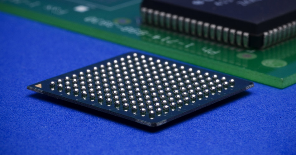
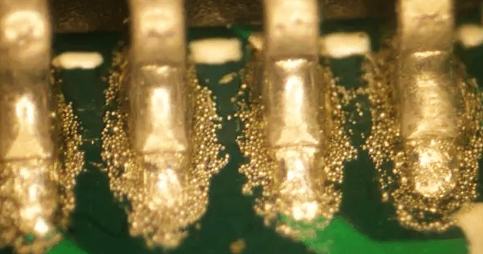
Manufacturing a chip on a wafer requires thousands of processes, and it takes more than three months from design to production. To remove the chip from the wafer, it is cut into a single chip with a diamond saw. These so-called "bare" chips are separated from 12 inch wafers, which are the most commonly used size in semiconductor manufacturing. Due to different chip sizes, some wafers can contain thousands of chips, while others only contain dozens.
These bare crystals are then placed on a "substrate" that uses a metal foil to direct the input and output signals of the bare crystals to other parts of the system. Then we will cover it with a "soaking plate". The soaking plate is a small flat metal protective container with coolant inside to ensure that the chip can keep cool during operation.
It's just the beginning
Now, chips have become a part of your smartphone, TV, tablet computer and other electronic products. It may be the size of a thumb, but a chip can contain billions of transistors. For example, Apple's A15 bionic chip contains 15 billion transistors, which can perform 15.8 trillion operations per second.
Of course, semiconductor manufacturing involves more than these steps. Chips need to go through measurement, inspection, electroplating, testing and more. Every chip has to go through hundreds of such processes before becoming a part of electronic equipment.


抖音二維碼

Q Q二維碼

微信二維碼
點擊
然后
聯系
然后
聯系
電話熱線
13410863085Q Q

微信

- 郵箱