鑫景福致力于滿足“快速服務(wù),零缺陷,輔助研發(fā)”PCBA訂購單需求。


PCBA方案設(shè)計(jì)
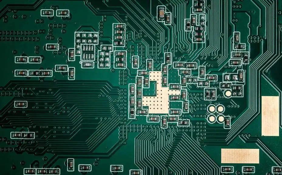
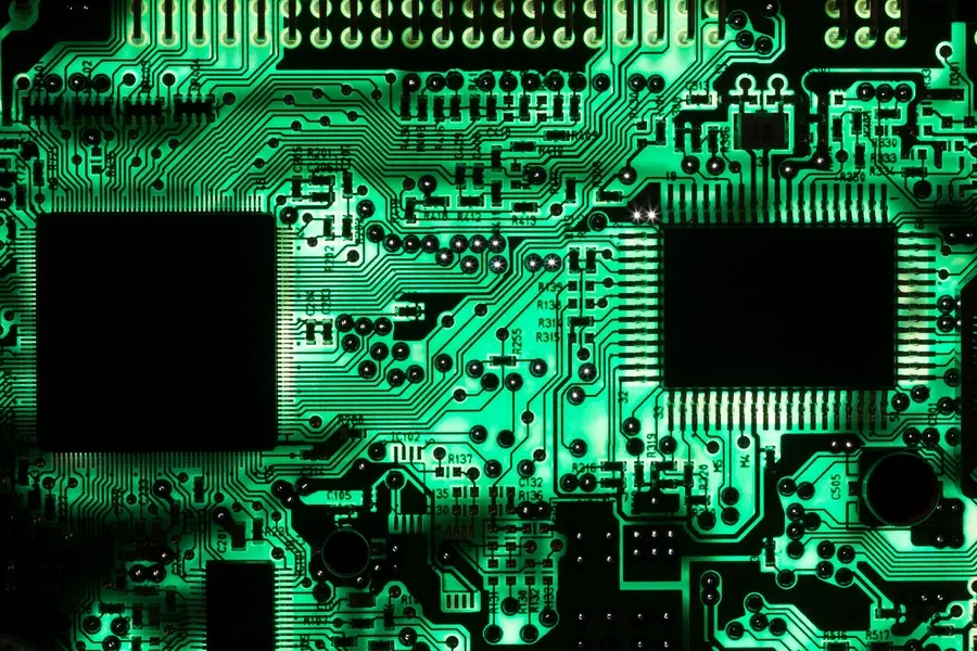
PCB process High speed PCB wiring attention
Q: What is the definition of high-speed system?
Answer: High speed digital signal is determined by the edge speed of the signal. It is generally believed that when the rise time is less than 4 tiMES the signal transmission delay, it can be regarded as a high speed signal. The high-frequency signal is usually used for signal frequency. The design and development of high-speed circuits should have the knowLEDge of signal analysis, transmission lines and analog circuits. Wrong concept: 8kHz frame signal is a low-speed signal.
Q: In the design of high-speed PCB, the automatIC wiring function is often needed. How can we effectively achieve automatic wiring?
A: In high-speed circuit boards, we can't just look at the speed and distribution rate of the router. At this time, we also need to see whether it can accept high-speed rules. For example, it is required that the length from the T-shaped contact to each terminal should be the same. At this time, CADence SPECCTRA can solve the high-speed wiring problem well. Many routers cannot receive or can only accept very few high-speed rules.
Q: In the design of high-Speed PCB, what is the relationship between crosstalk and the speed and direction of signal lines? What design indicators should be noted to avoid crosstalk and other problems?
Answer: Crosstalk will affect the edge rate. Generally speaking, when a group of buses have the same transmission direction, crosstalk will slow the edge rate. When the transmission direction of a group of buses is different, the crosstalk factor will make the edge rate faster. The crosstalk control can be realized by controlling the line length, line spacing, line stacking and source end matching. Q: For high-speed systems, what should be paid attention to when wiring multilayer circuit boards? What are the principles for defining the functions of each layer? Answer: Attention shall be paid to the arrangement of power supply and ground plane, and the wiring layer shall ensure consistent impedance. The key signals shall be laid on the route layer with plane layers on both sides as far as possible, and shall not be divided across the plane. It is generally determined according to the actual situation. The power supply and ground are connected to the power supply and ground by punching holes nearby.
Q: What measures can be taken to reduce the mutual interference between layers and improve the signal quality on a multilayer circuit board?
A: It is mainly to solve the problems of impedance control, matching, wiring return, power integrity, EMC, etc. Reducing the inter layer interference can reduce the distance between the routing layer and the plane layer, increase the distance between the routing layers, and try not to take parallel routing for adjacent routing layers. There are many methods, which cannot be listed one by one.
Q: How to divide digital power supply, analog power supply, digital ground and analog ground in PCB design?
Answer: The power supply is connected through the filter circuit, and the digital and analog are separated. Digital and analog circuits depend on specifIC chips. Some require separation, single point connection, and some do not need separation.
Q: The backplane only provides a ground, which is a digital ground. The card has both analog and digital parts. How to connect the analog ground?
A: According to the chip requirements of the analog part of the card, you can generally separate the digital and analog parts of the card, connect them at a single point on the card, and connect them digitally with the backplane.
Q: How to consider impedance matching in high-speed PCB design? In Multilayer circuit board design, how to calculate the characteristic impedance of the internal signal layer? How does the input impedance 50 Ω match the output impedance 75 Ω?
Answer: The impedance matching needs to be calculated according to the line width, line thickness, plate structure, etc. Sometimes, a series or parallel resistance must be added to achieve the matching. These parameters are also considered in the internal signal layer impedance calculation. The input impedance of 50 Ω and the output of 75 Ω cannot match completely, as long as the signal integrity and timing can be guaranteed.
Q: It is found in the EMC test that the harmonic of the clock signal exceeds the standard seriously. In addition to connecting the decoupling capacitor on the power supply pin, what other aspects should be paid attention to in PCB design to suppress electromagnetic radiation?
Answer: You can walk the clock signal in the inner layer, or connect a SMAll capacitor on the clock line to the ground (of course, it will affect the clock edge rate).
Vias and pads
a. The via can only be perforated on the inner wall (unless it is MARKed or the outer diameter is smaller than the inner diameter, it will be regarded as non porous by the manufacturer); The pad can be non porous directly (removing the check of Plated in Advanced of the pad is non porous).
b. The through hole is between the selected two layers, and the hole diameter cannot be 0. For multilayer boards, through holes, blind holes, and embedded holes can be made; The pad can only be in a single layer (via pad can also be considered as a single MultiLayer layer), the hole diameter can be 0, and the drill hole can only be a through hole.
c. The vias of the same network with copper cladding will be directly covered when copper cladding (the same network is selected); The pads with the same network as copper clad can be connected in an optional way.
d. The via can only be round; Pads can be square, rectangular, octagonal, circular, elliptical, etc. Pad Stack can be used to define the size and shape of the top layer, middle layer, and bottom layer.
Reliability Design of printed circuit board Decoupling Capacitor Configuration
In DC power supply circuit, the change of load will cause power supply noise. For example, in a digital circuit, when the circuit transitions from one state to another, a large SPIke current will be generated on the power line, forming a transient noise voltage. The configuration of decoupling capacitor can suppress the noise generated by load change, which is a conventional method for reliability design of printed circuit board. The configuration principles are as follows:
● The power input terminal is connected with an electrolytic capacitor of 10~100uF. If the position of the printed circuit board allows, the anti-interference effect of the electrolytic capacitor of more than 100uF will be better.
● Configure a 0.01uF ceramic capacitor for each integrated circuit chip. If the space of the printed circuit board is too small to fit, a 1~10uF tantalum electrolytic capacitor can be configured for every 4~10 chips. The high-frequency impedance of this device is very small. The impedance is less than 1 Ω in the range of 500kHz~20MHz, and the leakage current is very small (less than 0.5uA).
● For devices with weak noise capacity and large current change when turning off, and memory devices such as ROM and RAM, decoupling capacitors should be directly connected between the power line (Vcc) and ground wire (GND) of the chip.
● The lead of decoupling capacitor shall not be too long, especially the high frequency bypass capacitor shall not have lead
Fundamentals of Design PCB
10-30,2022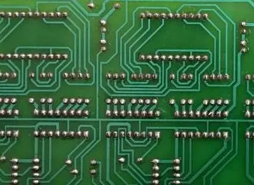


抖音二維碼

Q Q二維碼

微信二維碼
點(diǎn)擊
然后
聯(lián)系
然后
聯(lián)系
電話熱線
13410863085Q Q

微信

- 郵箱