鑫景福致力于滿(mǎn)足“快速服務(wù),零缺陷,輔助研發(fā)”P(pán)CBA訂購(gòu)單需求。


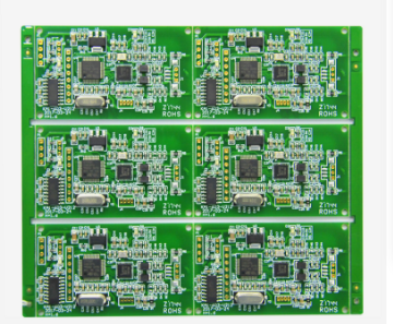
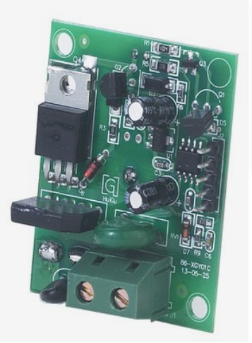
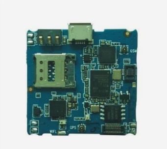
PCBA方案設(shè)計(jì)
In PCB circuit design, we generally care about the quality of the signal, but sometiMES we often limit our research to the signal line and treat the power and ground as an ideal situation. Although this can SIMplify the problem, it is no longer feasible in high-speed design. Although the direct result of circuit design is from the signal integrity, we must not neglect the power integrity design. Because the power supply integrity directly affects the signal integrity of the final PCB board. Power supply integrity and signal integrity are closely related, and in many cases, the main reason affecting signal distortion is the power supply system. For example, the ground bounce noise is too large, the design of decoupling capacitor is inappropriate, the loop impact is very serious, the division of multiple power sources/ground planes is not good, the stratum design is unreasonable, the current is uneven, and so on.

1) Power distribution system
Power integrity design is a very complex matter, but how to control the impedance between the power supply system (power supply and ground plane) is the key to the design in recent years. TheoretICally, the lower the impedance between power systems, the better. The lower the impedance, the SMAller the noise amplitude, and the smaller the voltage loss. In actual design, we can determine the target impedance we want to achieve by specifying the maximum voltage and power supply variation range, and then adjust the relevant factors in the circuit to approximate the target impedance (related to frequency) of each part of the power supply system.
2) Ground rebound
When the edge rate of high-speed devices is lower than 0.5ns, the data exchange rate from the large capacity data bus is particularly fast. When it generates strong ripples in the power layer that can affect the signal, the power supply will be unstable. When the current through the ground loop changes, a voltage will be generated due to the loop inductance. When the rising edge shrinks short, the current change rate increases, and the ground bounce voltage increases. At this time, the ground plane (ground wire) is not the ideal zero level, and the power supply is not the ideal DC potential. When the number of simultaneously opened and closed gate circuits increases, the ground bounce becomes more serious. For a 128 bit bus, there may be 50_ 100 I/O lines switch at the same clock edge. At this time, the inductance of the power supply and ground loop fed back to the I/O driver switched at the same time must be as low as possible, otherwise, a voltage brush will appear at a standstill connected to the same ground. Ground bounce can be seen everywhere, such as on chips, packages, connectors or PCB circuit boards, which may cause power integrity problems.
From the perspective of the development of PCB technology, the rising edge of devices will only be reduced, and the width of the bus will only be increased. The only way to keep the ground bounce acceptable is to reduce the power and ground distribution inductance. For a chip, it means moving to an array chip, placing as much power and ground as possible, and connecting wires to the package as short as possible to reduce inductance. For packaging, it means moving layer packaging to make the ground plane spacing of power supply closer, such as that used in BGA packaging. For connectors, it means using more ground pins or redesigning connectors to have internal power and ground planes, such as connector based ribbon cords. For the circuit board, it means to make the adjacent power supply and ground plane as close as possible. Since inductance is proportional to length, ground noise will be reduced if connection between power supply and ground is as short as possible.
3) Decoupling capacitor
We all know that adding some capacitors between the power supply and the ground can reduce the system noise, but how many capacitors are added to the circuit board? What is the appropriate capacitance value of each capacitor? Where is each capacitor better placed? We generally haven't considered these problems seriously, but only rely on the experience of PCB designers, sometimes even think that the less the capacitance, the better. In high-speed design, we must consider the parasitic parameters of capacitance, quantitatively calculate the number of coupling capacitors, the capacitance value of each capacitor and the specific location of each capacitor, to ensure that the impedance of the system is within the control range. A basic principle is that no decoupling capacitor is required, and no redundant capacitor is required.


抖音二維碼

Q Q二維碼

微信二維碼
點(diǎn)擊
然后
聯(lián)系
然后
聯(lián)系
電話(huà)熱線(xiàn)
13410863085Q Q

微信

- 郵箱