鑫景福致力于滿足“快速服務,零缺陷,輔助研發”PCBA訂購單需求。


PCBA方案設計
In addition to the selection of PCB components and circuit design, a good printed circuit board (PCB) design is also a very important factor in electromagnetic compatibility. The key to PCB EMC design is to reduce the reflow area as much as possible and let the reflow path flow in the designed direction. The most common return current problems come from the cracks in the reference plane, the transformed reference plane layer, and the signals flowing through the connector. Jumping capacitors or decoupling capacitors may solve some problems, but the overall impedance of capacitors, vias, pads and wiring must be considered. This lecture will introduce EMC technology from three aspects: PCB layering strategy, layout skills and routing rules.
PCB layering strategy
In circuit board design, thICkness, via process and number of layers of circuit board are not the key to solve the problem. Excellent layered stacking is the key to ensure bypass and decoupling of power bus, minimize the transient voltage on the power layer or ground layer, and shield the electromagnetic field of signal and power supply. From the point of view of signal routing, a good layering strategy should be to place all signal routing on one or several layers, which are close to the power layer or ground layer. For power supply, a good layering strategy should be that the power layer is adjacent to the ground plane, and the distance between the power layer and the ground plane should be as SMAll as possible. This is what we call "layering" strategy. Next, we will talk about the excellent PCB layering strategy.
1. The projection plane of the wiring layer should be within the area of its return plane layer. If the wiring layer is not within the projection area of its return plane layer, there will be signal lines outside the projection area during wiring, causing the "edge radiation" problem, and also increasing the area of the signal loop, leading to increased differential mode radiation.
2. Try to avoid setting adjacent wiring layers. Because parallel signal routing on adjacent wiring layers will cause signal crosstalk, if it is impossible to avoid adjacent wiring layers, the layer spacing between the two wiring layers should be appropriately increased to reduce the layer spacing between the wiring layers and their signal loops.
3. The projection planes of adjacent plane layers shall not overlap. Because when the projection overlaps, the coupling capacitance between layers will cause the noise between layers to be coupLED.
Multilayer board design:
When the clock frequency exceeds 5MHz or the signal rise time is less than 5ns, in order to control the area of the signal loop well, it is generally necessary to use a multilayer Board Design. The following principles should be paid attention to when designing multilayer boards:
1. The key wiring layer (the layer where clock line, bus, interface signal line, radio frequency line, reset signal line, chip selection signal line and various control signal lines are located) shall be adjacent to the complete ground plane, preferably between two ground planes. Key signal lines are generally strong radiation or extremely sensitive signal lines. Wiring close to the ground plane can reduce the area of its signal circuit, reduce its radiation intensity or improve its anti-interference capability.
2. The power supply plane shall be retracted relative to its adjacent ground plane (the recommended value is 5H~20H). Shrinking the power plane relative to its return ground plane can effectively suppress the "edge radiation" problem.
In addition, the main working power plane of the single board (the most widely used power plane) should be close to its ground plane to effectively reduce the loop area of the power supply current.
3. Whether there is no signal line ≥ 50MHz at the TOP and BOTTOM layers of the board. If so, it is better to walk the high-frequency signal between two plane layers to suppress its radiation to space.
Single and double deck design:
For the design of single-layer board and double-layer board, attention should be paid to the design of key signal lines and power lines. There must be ground wires adjacent to and parallel to the power supply wiring to reduce the area of the power supply current loop.
"Guide Ground Line" shall be laid on both sides of the key signal line of the single-layer board. The projection plane of the key signal line of the double-layer board should have a large area of flooring, or the same processing method as that of the single layer board, and the "Guide Ground Line" should be designed. The "guard ground wire" on both sides of the key signal line can reduce the area of the signal loop on the one hand, and can also prevent crosstalk between the signal line and other signal lines.
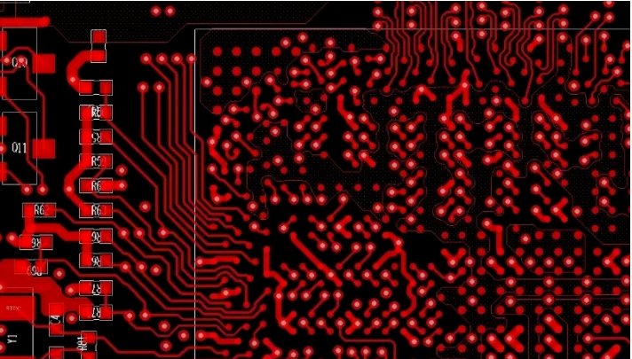
In general, PCB layering can be designed according to the following table.
PCB layout Skills
During PCB layout design, the design principle of straight line placement along the signal flow direction shall be fully followed to avoid looping back and forth as far as possible. This can avoid direct coupling of signals and affect signal quality. In addition, in order to prevent mutual interference and coupling between circuits and PCB components, the placement of circuits and the Layout of components should follow the following principles:
1. If the interface on the board is designed to be "clean", the filter and isolation devices should be placed on the isolation belt between the "clean" and the working place. This can avoid mutual coupling of filter or isolation devices through the plane layer and weaken the effect. In addition, no other devices except filter and protective devices can be placed on the "clean ground".
2. When multiple module circuits are placed on the same PCB, digital circuits and analog circuits, high-speed and low-speed circuits shall be arranged separately to avoid mutual interference between digital circuits, analog circuits, high-speed circuits and low-speed circuits. In addition, when there are high, medium and low speed circuits on the circuit board at the same time, in order to prevent high-frequency circuit noise from radiating outward through the interface.
3. The filter circuit of the power input port of the circuit board shall be placed close to the interface to prevent the filtered circuit from being coupled again.
4. The filtering, protection and isolation devices of the interface circuit are placed close to the interface, which can effectively achieve the effects of protection, filtering and isolation. If there are both filtering and protection circuits at the interface, the principle of protection before filtering shall be followed. Because the protection circuit is used for external overvoltage and overcurrent suppression, if the protection circuit is placed behind the filter circuit, the filter circuit will be damaged by overvoltage and overcurrent. In addition, since the mutual coupling of the input and output wiring of the circuit will weaken the filtering, isolation or protection effects, the PCB layout should ensure that the input and output lines of the filtering circuit (filter), isolation and protection circuits are not coupled with each other.
5. Sensitive circuits or devices (such as reset circuits) shall be at least 1000 mil away from the edges of boards, especially the edges of board interfaces.
6. Energy storage and high-frequency filter capacitors shall be placed near unit circuits or devices with large current changes (such as input and output terminals of power modules, fans and relays) to reduce the loop area of large current loops.
7. Filter elements shall be placed side by side to prevent the filtered circuit from being interfered again.
8. Crystals, crystal oscillators, relays, switching power supplies and other strong radiation devices shall be at least 1000 mils away from the board interface connector. In this way, the interference can be radiated outward directly or the current can be coupled on the outgoing cable to radiate outward.
PCB wiring rules
In addition to the selection of components and circuit design, good PCB wiring is also a very important factor in EMC. Since PCB is an inherent component of the system, enhancing EMC in PCB wiring will not bring additional costs to the final completion of the product. Anyone should remember that a poor PCB wiring can lead to more EMC problems, rather than eliminate these problems. In many cases, even adding filters and components can not solve these problems. In the end, the entire board had to be rewired. Therefore, it is the most cost-effective way to develop good PCB wiring habits at the beginning. Some general rules of PCB wiring and design strategies of power line, ground line and signal line will be introduced below. Finally, according to these rules, improvement measures are proposed for typical PCB circuits of air conditioners.
1. Wiring separation
The function of wiring separation is to minimize crosstalk and noise coupling between adjacent lines in the same PCB layer. The 3W specification indicates that all signals (clock, video, audio, reset, etc.) are isolated from line to line, edge to edge. In order to further reduce the magnetic coupling, the reference ground is placed near the key signal to isolate the coupling noise generated on other signal lines.
2. Protection and shunt line
Setting shunt and protection lines is a very effective method to isolate and protect key signals, such as system clock signals in a noisy environment. Parallel or protection lines in PCB are laid along the lines of key signals. The protection line not only isolates the coupling magnetic flux generated by other signal lines, but also isolates the key signals from the coupling with other signal lines. The difference between the shunt line and the protection line is that the shunt line does not have to be terminated (connected to ground), but both ends of the protection line must be connected to ground. In order to further reduce the coupling, the protective circuit in the multilayer PCB can add a path to the ground every other section.
3. Power cord design
According to the current of the printed circuit board, the width of the power line shall be thickened as much as possible to reduce the loop resistance. At the same time, make the direction of power line and ground wire consistent with the direction of data transmission, which helps to enhance the anti noise ability. In the single panel or double sided panel, if the power line runs very long, the decoupling capacitance should be added to the ground every 3000mil, and the capacitance value is 10uF+1000pF.
4. Ground wire design
The principle of ground wire design is:
(1) Separated digitally from analog. If there are both logic circuits and linear circuits on the circuit board, they should be separated as far as possible. The grounding of low-frequency circuit shall adopt single point parallel grounding as far as possible. If the actual wiring is difficult, part of the circuit can be connected in series and then connected to the ground in parallel. High frequency circuit should adopt multipoint series grounding, the ground wire should be short and leased, and grid shaped large area ground foil should be used around high-frequency components as far as possible.
(2) The grounding wire shall be thickened as much as possible. If the ground wire is sewn, the ground potential will change with the change of current, which will reduce the noise resistance. Therefore, the grounding wire should be thickened so that it can pass three tiMES the allowable current on the printed board. If possible, the grounding wire should be more than 2~3mm.
(3) The grounding wire forms a closed loop. For printed circuit board composed of digital circuits only, the grounding circuit of the printed circuit board is arranged into a group loop, which can improve the anti noise ability.
5. Signal line design
For key signal lines, if the board has an internal signal routing layer, the clock and other key signal lines are laid in the inner layer, and the routing layer is preferred. In addition, the key signal lines must not be routed across the partition area, including the reference plane gap caused by vias and pads, otherwise the area of the signal circuit will increase. Moreover, the distance between the key signal line and the edge of the reference plane shall be ≥ 3H (H is the height of the line from the reference plane) to suppress the edge radiation effect.
The clock line, bus, radio frequency line and other strong radiation signal lines and the reset signal line, chip selection signal line, system control signal and other sensitive signal lines should be far away from the interface outgoing signal line. Thus, the interference on the strong radiation signal line can not be coupled to the outgoing signal line and radiate outwards; It also prevents the external interference brought in by the outgoing signal line of the interface from coupling to the sensitive signal line, which may lead to system misoperation.
The differential signal lines shall be routed in the same layer, equal length and parallel to keep the same impedance, and there shall be no other routing between the differential lines. Because the common mode impedance of the differential line pair is equal, its anti-interference ability can be improved.
According to the above PCB wiring rules, the typical PCB circuit of the air conditioner is improved and optimized.


抖音二維碼

Q Q二維碼

微信二維碼
點擊
然后
聯系
然后
聯系
電話熱線
13410863085Q Q

微信

- 郵箱