鑫景福致力于滿足“快速服務,零缺陷,輔助研發”PCBA訂購單需求。


PCBA方案設計
PCB design process
PCB rule setting
The unit of the design rule follows the unit set in the canvas property, where the unit is mil. The minimum wire width of conductor is 10mil; The minimum distance between different network elements is 8mil; The outer diameter of the hole is 24mil, and the inner diameter of the hole is 12ml; The line length is not set; During PCB design, the functions of "real-time rule detection", "distance from detection element to copper coating" and "DRC safe boundary display during wiring" should be enabLED.
PCB design
Layout principle
The layout shall generally comply with the following principles:
(1) Principle of shortest wiring. For example, the decoupling capacitor of integrated circuit (IC) should be placed at the corresponding VCC and GND as far as possible
Between pins, and as close as possible to the IC, so as to form the shortest loop with VCC and GND.
(2) The principle of centralizing the same functional module. That is, the components in the relevant circuit modules that achieve the same function are distributed nearby
Bureau.
(3) Follow the principle of "large before SMAll, difficult before easy", that is, the layout of important unit circuits and core components should be given priority.
(4) The layout shall refer to the schematic diagram and arrange the main components according to the main signal flow direction of the circuit.
(5) The arrangement of components shall be convenient for debugging and maintenance, that is, large components cannot be placed around small components, and there shall be enough space around components to be debugged.
(6) Plug in components of the same type shall be placed in one direction in the X or Y direction. Polarized discrete components of the same type shall also be kept consistent in the X or Y direction as far as possible to facilitate production and inspection.
(7) During layout, the distance between the components located at the edge of the circuit board and the edge of the circuit board is generally not less than 2mm. If space allows, it is recommended to keep the distance at 5mm.
(8) The crystal oscillator shall be arranged as close to the IC as possible, and the capacitor connected to the crystal oscillator shall be close to the crystal oscillator.
Wiring Precautions
Pay attention to the following when wiring:
(1) In principle, the power trunk line should be thickened (especially the power input/output line of the circuit board).
(2) PCB wiring shall not be too close to the positioning hole and the circuit board frame, otherwise, the wire can be easily cut off or even cut off during PCB drilling.
(3) 90 ° corner wiring is prohibited on the same layer, but 90 ° wiring through holes between different layers is allowed. In addition, the principle of horizontal wiring on one layer and vertical wiring on the other layer shall be followed when wiring.
(4) High frequency signal lines, such as the wiring of crystal oscillator circuit on the STM32 core board, should not be thickened. It is recommended that the line width should also be designed as 10mil, and the wiring should be on the same layer as far as possible.
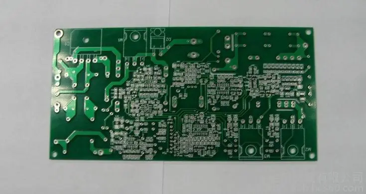
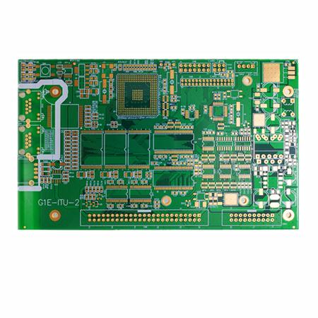
PCB multilayer circuit board proofing requirements
Nowadays, the use of PCB multilayer circuit boards has become a popular trend in the MARKet, and in the development of the industry, many PCB manufacturers have become increasingly prominent in the ability to develop and produce PCB multilayer circuit boards. So, what are the requirements for the proofing of PCB multilayer circuit boards? Now, I will analyze for you:
1. Requirements for neat appearance. During PCB multi-layer circuit board proofing, the appearance of the sample plate shall be flat, the corners shall be free of burrs, and there shall be no blistering and delamination between the wire and the solder mask. Only in this way can PCB multilayer circuit boards ensure better welding effect, and also ensure that PCB multilayer circuit boards produced by PCB manufacturers meet the appearance requirements of actual use.
2. Requirements for reasonable process. Before proofing, PCB multilayer circuit board also needs to study whether its process is reasonable, such as whether there is mutual interference between lines, to ensure that PCB multilayer circuit board can run stably for a long time.
3. CAM optimization requirements. In order to obtain high-quality PCB multilayer circuit boards, relevant CAM processing is required during proofing. This processing includes adjusting the line width, optimizing the spacing and bonding pads, etc., to ensure that the circuit interaction between PCB multilayer circuit boards has good signals, so that the quality of the template is more superior.
The above are the basic requirements for PCB multilayer circuit board proofing. High quality proofing can enable PCB multilayer circuit board to have higher quality, and mass production can be carried out after ensuring that the quality is correct. Therefore, reasonable design planning of PCB multilayer circuit board according to requirements is also for better production of PCB multilayer circuit board.


抖音二維碼

Q Q二維碼

微信二維碼
點擊
然后
聯系
然后
聯系
電話熱線
13410863085Q Q

微信

- 郵箱