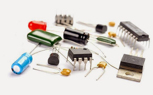
鑫景福致力于滿足“快速服務,零缺陷,輔助研發”PCBA訂購單需求。


PCBA方案設計
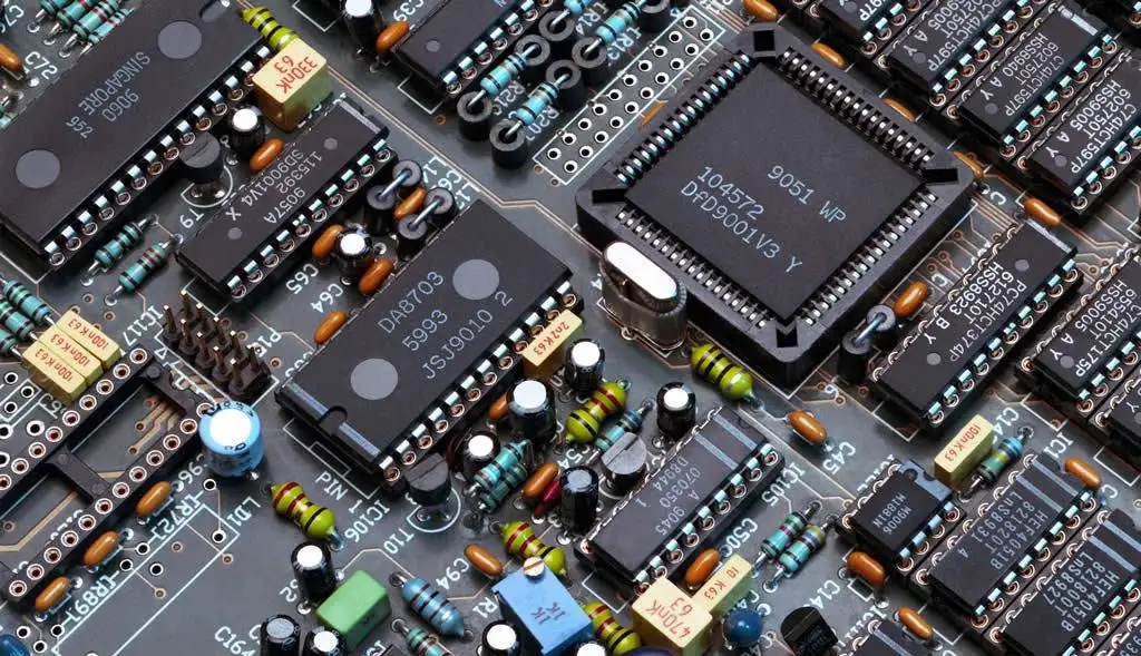
DetaiLED explanation of basIC rules of component layout for PCB layout
1. The layout shall be carried out according to the circuit modules, and the relevant circuits realizing the same function shall be called a module. The components in the circuit modules shall be centralized nearby, and the digital circuits and analog circuits shall be separated;
2. Elements and devices shall not be mounted within 1.27mm around non mounting holes such as positioning holes and standard holes, and components shall not be mounted within 3.5mm (for M2.5) and 4mm (for M3) around mounting holes such as screws;
3. Avoid laying vias under horizontally installed resistors, inductors (plug-ins), electrolytic capacitors and other components to avoid short circuit between vias and component shells after wave soldering;
4. The distance from the outer side of the components to the board edge is 5mm;
5. The distance between the outer side of the mounting element pad and the outer side of the adjacent plug-in elements is greater than 2mm;
6. The metal shell components and metal parts (shielding box, etc.) shall not collide with other components, and shall not be close to the printed wire and bonding pad. The distance between them shall be greater than 2mm. The distance from the outside of positioning hole, fastener mounting hole, elliptical hole and other square holes in the plate to the plate edge is greater than 3mm;
7. The heating element shall not be close to the conductor and thermal element; High heat devices should be evenly distributed;
8. The power socket shall be arranged around the printed board as much as possible, and the terminal of the power socket and its connected bus bar shall be arranged on the same side. Special attention shall be paid not to arrange power sockets and other welding connectors between connectors, so as to facilitate the welding of these sockets and connectors and the design and wiring of power cables. The spacing of power sockets and welding connectors shall be arranged to facilitate the plugging and unplugging of power plugs;
9. Layout of other components: All IC components are aligned on one side, and polarity MARKs of polar components are clear. The polarity marks on the same printed board shall not be more than two directions. When there are two directions, the two directions are perpendicular to each other;
10. The wiring on the board surface shall be properly densified. When the density difference is too large, it shall be filled with MESh copper foil, and the mesh shall be greater than 8mil (or 0.2mm);
11. There shall be no through-hole on the SMD pad to prevent the loss of solder paste from causing faulty soldering of components. Important signal lines are not allowed to pass through the socket pins;
12. The patch is aligned on one side, with consistent character direction and packaging direction;
13. Polarized devices shall be in the same direction as far as possible with polarity marks on the same board.
PCB manufacturers, PCB designers and PCBA manufacturers will explain the basic rules of component layout for PCB layout.


抖音二維碼

Q Q二維碼

微信二維碼
點擊
然后
聯系
然后
聯系
電話熱線
13410863085Q Q

微信

- 郵箱