鑫景福致力于滿足“快速服務(wù),零缺陷,輔助研發(fā)”PCBA訂購單需求。


PCBA方案設(shè)計(jì)
PCB board level mask cavity analysis and system design and development
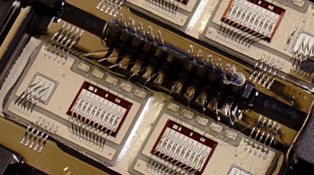
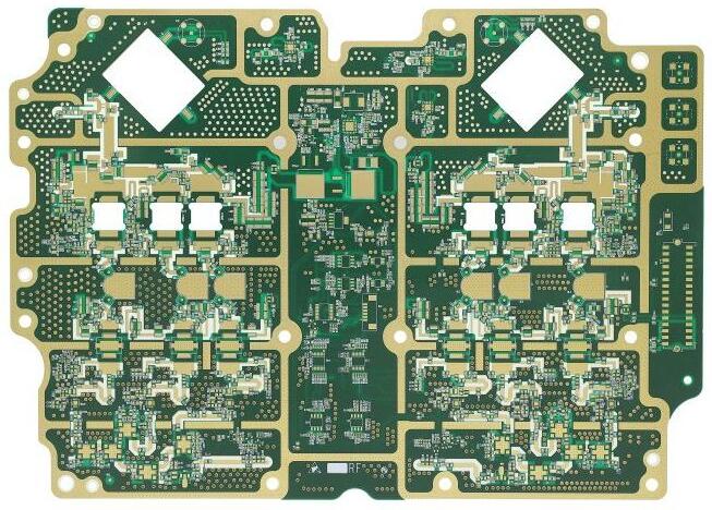
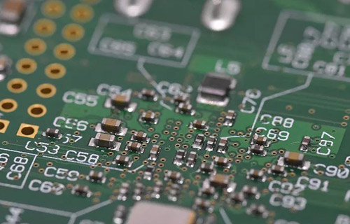
Printed circuit board or PWB (printed wiring board) is arranged to replace the chassis of the previous electronIC components and realize the interconnection between electronIC components Because this board is printed electronically, it is calLED a "printed" circuit board It is inaccurate to refer to "printed circuit board" as "printed circuit board", because there is no "printed element" on the printed circuit board, only wiring The installation method used, the planned test and inspection method, and the layout of printed circuit boards and components are key issues The design of printed circuit board is based on the circuit schematic diagram to realize the functions required by the circuit designer PCB design mainly refers to layout design, which needs to consider various factors, such as the layout of external connections, the optimal layout of internal electronic components, the optimal layout of metal connectors and through holes, electromagnetic protection, and heat dissipation Layout design can save production cost and achieve good circuit efficiency and heat dissipation efficiency SIMple layout design needs to be realized by computer aided design (CAD) Just like the power supply selection, the decision to select the RF interference mask cavity is usually made during the design process. There is usually not enough space to add the mask cavity, causing the cavity to have a physical impact on other areas of the design
Printed circuit board

3DS Design, Development, Draw
The design and development of PCB - level mask cavity and system can be summarized into three key steps: design, development, and drawing Active communication and negotiation between cavity users and cavity design team is crucial Look for cavity manufacturers who can provide preliminary design guidance, use suggestions, site visits, prototype design, sample production, paint and thickness selection, machining, assembly, and reassess cost savings In order to obtain MARKet profitability of products, cost must be limited The combination of structural design, detailed design and customer input can achieve the expected goal of "achieving the expected results at a limited cost"
Form choice
When choosing the type of activity to use, many factors must be considered What on earth is blocked? What is the exact nature of the masked interference source? After installing the cavity on the PCB, does the customer still need to open the cavity for modification, testing, inspection or adjustment? Does the output match the machine placement cost? Which loop areas need to be masked or isolated from other areas? Should one chamber or multiple chambers be used in this application? Will the final product be subjected to impact test, vibration test or package drop test?
shielded form
For a particular application, careful consideration of the above issues will help to select an appropriate and economical mask form Different four sided mask cavities can be selected according to different application requirements If the height of the fence is high enough to accommodate the finger spring, the finger spring cover is an option in the removable cover If there is not enough space outside the fence for an external finger spring, an internal finger spring shall be used In addition, external and internal finger springs of the same shape can be mixed on the opposite side The surface mounted tetrahedron chamber with finger spring is another option for the mask chamber This type of cavity is the same as the ordinary tetrahedron cavity, except there is no fixing pin Seam welding is usually used to weld it to PCB along a continuous path This may require the use of a stamped fence structure Planar folding cover can also be used for quadrangular PCB cavity, as shown in Figure 2 This type of lid has low production cost, especially in the development phase The disadvantage of this design is that the effective connection between the cover and the fence cannot be guaranteed unless the cover is used to fix the label Any gap in the connection will affect the EMC performance of the cavity The cover retaining strip can be folded or wrapped, as shown in Figures 2 and 3 These two types of stickers can be used for more than 5 tiMES of movement and cover replacement
Flat Folding Lid
Snap-on lids can be used when the actual application requires the fence and lid to have a low profile. The projection on the side wall of the cover is inserted into the SMAll seam of the side wall of the fence This design option reduces the height of the fence to 1.5 mm As with the selection of labels and slot covers, this design does not guarantee an effective connection between the fence and the cover unless small pieces are used to fix the position Some designers prefer to use surface mount line placement equipment to integrate the cover and fence Only open the lid when reworking components in the cavity Selecting this design means that a row of small holes must be left on the cover so that heat can enter the chamber to weld the internal electronic components to the PCB, as shown in Figure 4 Unfortunately, these holes will reduce the mask efficiency of the chamber by about 20dB When installing the cavity after the test, or when the PCB board is large, it is more cost-effective to choose a five sided cavity This option can be realized by welding pins, spot welding or butt welding, or machining through hot return holes Up to now, the cost-effective way to develop and produce a small number of pentahedral cavities is to select a curved pentahedral cavity As shown in Figure 5, this is achieved by adding a logo on the plate When installing it on a PCB, the user only needs to fold it into the desired shape
Shielding material
For most RF shielding, the mask layer can be made of almost any substrate, such as copper, brass, stainless steel, aluminum or nickel brass The installation process of soldering components to the printed circuit board is more electroplated than nickel brass Traditionally, bright tin plating has been used However, with the implementation of RoHS directive, PCB production line has been changed to lead-free soldering Low frequency interference is usually caused by magnetic fields Although sometimes thicker steel plates or phOSPhor bronze are used to make the mask cavity, more special information, such as metal or radio frequency information, is used to make the mask cavity The frequency limit of metal film mask cavity is generally 3~5GHz If this frequency range is exceeded, both effects limit mask performance or its effectiveness Due to the distributed capacitance between the cavity and the electronic components on the PCB, any slight movement in the cavity metal will produce a micro sound effect In this frequency band, the protective cover is usually machined in solid form to overcome the above effects It is possible that under the harmonic frequency of the working frequency of the loop, the cavity of the cavity becomes a part of the waveguide, where another high-frequency effect occurs This effect makes the cavity behave more like a resonator than a mask This effect can be avoided by adding absorption data to the cavity or by carefully selecting the cavity size
Production and Assembly Design
A key factor in cavity design is knowing the throughput of the final part or product. This judgment will determine the choice of production method and, to some extent, the choice of mask form As mentioned above, with the fence cover design and five sided cavity, it is obviously cheaper to produce a single piece than to combine two pieces to form a mask The selected production method also affects component costs For example, compare the cost of photographic machine (PCM) versus stamping or a combination of the two methods Are components installed manually or by machine? If machine installation is used, since most machines use vacuum suction heads to pick up components, it is necessary to place targets Some machines use a clamp type system to pick up parts, which is rare For machine installation, the coplanar PCB of the edge fence is required to be greater than 0.1mm to ensure that the cavity is on the solder paste when installing or entering the reflow soldering furnace
Machined General Shielding Materials
For most RF shielding, the mask layer can be made of almost any substrate, such as copper, brass, stainless steel, aluminum or nickel brass The installation process of soldering components to the printed circuit board is more electroplated than nickel brass Low frequency interference is usually caused by magnetic fields Although sometimes thicker steel plates or phosphor bronze are used to make the mask cavity, more special information, such as metal or radio frequency information, is used to make the mask cavity The frequency limit of metal film mask cavity is generally 3~5GHz If this frequency range is exceeded, both effects limit mask performance or its effectiveness Due to the distributed capacitance PCB between the cavity and the electronic components, any slight movement in the cavity metal will produce a micro sound effect


抖音二維碼

Q Q二維碼

微信二維碼
點(diǎn)擊
然后
聯(lián)系
然后
聯(lián)系
電話熱線
13410863085Q Q

微信

- 郵箱