鑫景福致力于滿足“快速服務,零缺陷,輔助研發”PCBA訂購單需求。


PCBA方案設計

Encyclopedia of PCB failure Analysis
As the carrier of various components and the hub of circuit signal transmission, this PCB has become an important and key part of electronIC information products Its quality and reliability determine the quality and reliability of the whole equipment However, due to cost and scientific and technological reasons, a large number of faulty PCB boards have appeared in production and application For this kind of fault problem, we need to use some common fault analysis technologies to ensure that PCB boards are manufactured This paper summarizes ten kinds of fault analysis technology for reference
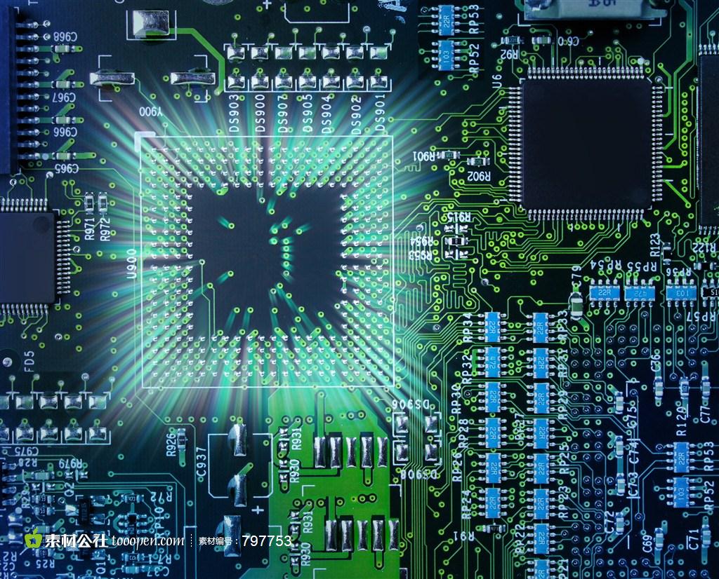
Circuit board

1. Visual inspection
A. appearance inspection is to inspect the ppearance of the PCB or use some SIMple instruments, such as stereoscopic microscope, metallographic microscope and even magnifying glass, to find the fault location and relevant physical evidence The main function is to locate the fault and preliminarily determine the PCB board The appearance inspection mainly checks the PCB board for contamination, corrosion, location of broken boards, circuit wiring and failure rules. If it is batch or single, it is always concentrated in a certain area, etc In addition, many PCB boards have been assembLED only in PCB board A Whether the fault is caused by the assembly process and the data used in the process, it is also necessary to carefully check the characteristics of the fault area
2. X-ray fluoroscopy
For some parts that cannot be visually inspected, and PCB boards must be inspected with X-ray fluoroscopy system The X-ray fluoroscopy system uses different data thicknesses or different data densities for imaging according to different principles of X-ray moisture absorption or transmittance This technology is more used to check PCB A solder joints, through hole internal defects, and BGA or CSP device defect solder joints in high-density packaging At present, the resolution of industrial X-ray fluoroscopy equipment can reach 1 μ m or less, and it is changing from two-dimensional imaging equipment to three-dimensional imaging equipment There are even five dimensional (5D) equipment used for package inspection
3 Slice analysis
Slicing analysis is the process of observing the cross sectional structure of the PCB through a series of methods and steps such as sampling, inlaying, slicing, polishing, corrosion, and observation Through slice analysis, we can obtain rich microstructure information PCB (through holes, electroplating, etc.) that reflects the quality of data, which provides a good basis for the next step of quality improvement However, this approach is destructive Once sliced, the sample will inevitably be destroyed; At the same time, this method requires a large number of samples and takes a long time to prepare samples, which requires well-trained scientific and technical personnel to complete For detailed slicing process, please refer to IPC standards IPC-TM-650 2.1.1 and IPC-MS-810
4. Scanning acoustic microscope
At present, C-mode ultrasonic scanning acoustic microscope is mainly used for electronic packaging or assembly analysis It uses amplitude and high-frequency ultrasound to reflect phase and polarity changes on discontinuous interfaces of data and images The scanning method is to scan the information on the X-Y plane along the Z-axis Therefore, the scanning acoustic microscope can be used to detect components, data, and various internal defects of PCB and PCB A, including cracks, delaminations, inclusions, and cavities If the scanning acoustic frequency width is sufficient, the internal defects of the solder joint can also be directly detected Typical scanning acoustic images use a red warning color to indicate the presence of defects Because a large number of plastic packaging components are used in the SMT process, there are a lot of water reflux sensitivity problems in the conversion process from lead to lead-free That is to say, when the lead-free process temperature is high, moisture absorbing plastic packaging devices will have internal or substrate delamination cracks during reflow, and ordinary pcb boards will often burst under the high temperature of lead-free process At this time, the scanning acoustic microscope highlighted its special advantages in multi-layer high-density nondestructive testing PCB boards In general, visible bursts can only be detected by visual inspection
5. Micro-infrared analysis
Micro-infrared analysis is an analysis method that combines infrared spectroscopy and microscope. It uses the principle of different absorption of infrared spectrum by different material (mainly organic material) to analyze the compound composition of the material Combined with a microscope, visible light and infrared light can be the same Light path, as long as it is within the visible field of vision, you can find the trace organic pollutants to be analyzed Without the combination of microscopes, infrared spectroscopy usually can only analyze a large number of samples However, in many cases, in the field of electronic technology, micro contamination may lead to poor solderability of PCB pads or lead pins It can be imagined that without the infrared spectrum of the microscope, it is difficult to solve the process problem The main purpose of micro infrared analysis is to analyze the organic pollutants on the welding surface or solder joint surface, and analyze the causes of corrosion or poor weldability
6. Scanning electron microscope analysis
Scanning electron microscope (SEM) is a useful large-scale electron microscopy imaging system for failure analysis. Its working principle is to accelerate the electron beam EMItted by the cathode by the anode, and form a beam with a diameter of tens to tens after being focused by the magnetic lens A thousand and Angstroms (A) of electron beam, when the scanning coil is deflected, the electron beam scans the sample surface point by point in a certain time and space sequence This high-energy electron beam bombards the sample surface and will stimulate various information, which can be collected and amplified to obtain various corresponding graphics from the display The excited secondary electrons are generated within 5-10nm of the sample surface Therefore, secondary electrons can better reflect the morphology of the sample surface; The excited backscattered electrons are generated on the sample surface 100, and the range is about 1000 nm. The backscattered electrons with different characteristics are emitted according to the atomic number of the material Therefore, the backscattered electron image has morphological characteristics and the ability to distinguish atomic numbers Therefore, the backscattered electron image can reflect the composition and distribution of chemical elements The current scanning electron microscope has a very powerful function. Any fine structure or surface feature can be magnified hundreds of thousands of tiMES for observation and analysis In fault analysis, scanning electron microscopy (SEM) is mainly used to analyze the failure mechanism of PCB or solder joint Specifically, it is used to observe the topographical structure of the pad surface, the metallographic structure of the solder joint, and measure the intermetallic compound and solderability Coating analysis and tin whisker analysis and measurement Unlike optical microscopes, scanning electron microscopes produce electronic images, so only black and white are produced The sample of scanning electron microscope needs conductivity Non conductors and some transistors need to be sprayed with gold or carbon Otherwise, the accumulation of surface charge of the sample will affect the observation of the sample In addition, the image of scanning electron microscope is more profound than the field depth of optical microscope. It is an important analysis method for inhomogeneous samples such as metallography, micro fracture and tin whisker
7. X-ray energy spectrum analysis
The scanning electron microscope mentioned above is generally equipped with an X-ray energy spectrometer. When the high energy electron beam hits the sample surface, the internal electrons in the surface matter atoms are bombarded and escape When the outer electron transitions to a lower energy level, the characteristic X-ray will be excited Characteristics of different atomic energy levels emitting different elements X-rays are different Therefore, the characteristic X-ray emitted by the sample can be used as a chemical component for analysis At the same time, the corresponding instruments are called spectral dispersion spectrometer (abricated as spectrometer (WDS) and energy dispersion spectrometer (abricated as energy spectrometer (EDS)) according to the detected X-ray signal as the characteristic wavelength or characteristic energy. The resolution of the spectrometer is higher than that of the energy spectrometer, and the analysis speed of the energy spectrometer is faster than that of the spectrometer Because of its high speed and low cost, the scanning electron microscope is usually equipped with an energy spectrometer With different electron beam scanning methods, the energy spectrometer can perform surface point analysis, circuit analysis, and surface analysis, and can obtain information about the different distribution of elements Point analysis obtains all elements of a point; Line analysis executes one element analysis on the specified line each time, and scans multiple times to obtain the line distribution of all elements; Surface analysis analyzes all elements in the specified surface, and the content of measured elements is the average value of the measured surface range In the analysis of PCB boards, the energy spectrometer is mainly used for the composition analysis of the pad surface and the element analysis of surface contaminants with poor solderability of pads and lead pins The accuracy of quantitative analysis of energy spectrometer is limited, and the content is less than 0.1%, which is usually not easy to detect The combination of energy spectrum and scanning electron microscopy can obtain both surface morphology and composition information, which is why they are widely used


抖音二維碼

Q Q二維碼

微信二維碼
點擊
然后
聯系
然后
聯系
電話熱線
13410863085Q Q

微信

- 郵箱