鑫景福致力于滿足“快速服務,零缺陷,輔助研發”PCBA訂購單需求。


PCBA方案設計

Cause Analysis of PCB copper Wire Falling off
Reason 1. PCB copper foil falls off due to PCB manufacturer's process factors
PCB copper foil is over matched. At present, the electrolytIC copper foil used in PCB factories is usually single-sided zinc plating (commonly referred to as ashing foil) and single-sided copper plating. (commonly known as red foil), common copper foil falling off are galvanized copper foil above 70um, red foil and ashed copper foil below 18um, and basically there is no large copper foil falling off. When the customer's PCB line design is superior to the etching line, if the copper foil specification changes and the etching parameters remain unchanged, the copper foil will stay in the etching solution for too long. Zinc was originally an active metal. When the copper wire on the PCB is immersed in the etching solution for a long time, it will cause excessive etching of the circuit, which will cause the zinc layer on the back of some thin wires to completely react and separate from the substrate, that is, the copper wire will fall off. Another situation is that the PCB etching parameters are very good, but after etching, the copper wire is poorly cleaned and dried, resulting in the copper wire being surrounded by etching solution residues on the transient surface of the PCB. If it is not treated for a long time, the copper wire will be over matched and the copper foil will fall off. This situation is usually manifested as concentrated on thin lines, or in wet weather, SIMilar adverse effects will occur on the entire PCB. Strip the copper wire to see if its color changes with the substrate contact surface (the so-calLED roughened surface). Different from the normal copper foil color, the original copper foil color at the bottom is visible, and the peel strength of the copper foil at the thick line is also normal.

2. Local collision occurs during PCB production, and the copper wire is separated from the substrate by mechanical external force. This is manifested by poor positioning or directivity, obvious twisting of dropped copper wires, or scratches/impact MARKs in the same direction. If you observe the copper foil surface after peeling off the defective parts, you can see that the color of the copper foil surface is normal, there is no bad side etching, and the peel strength of the copper foil is normal.
3. Generally, as long as the high temperature part of PCB exceeds 30 minutes after hot pressing, the copper foil and the sEMI solidified board will be completely combined, and this combination will not affect the binding force of the copper foil and the substrate in PCB. But they overlap on the laminate. In the process of stacking, if PP is polluted or the copper foil surface is damaged, the bonding force between the copper foil and the substrate after lamination will also be insufficient, resulting in the falling off of positioning (only applicable to large plates) or scattered copper wires, but the copper foil will not have abnormal peeling strength near the stripping line.
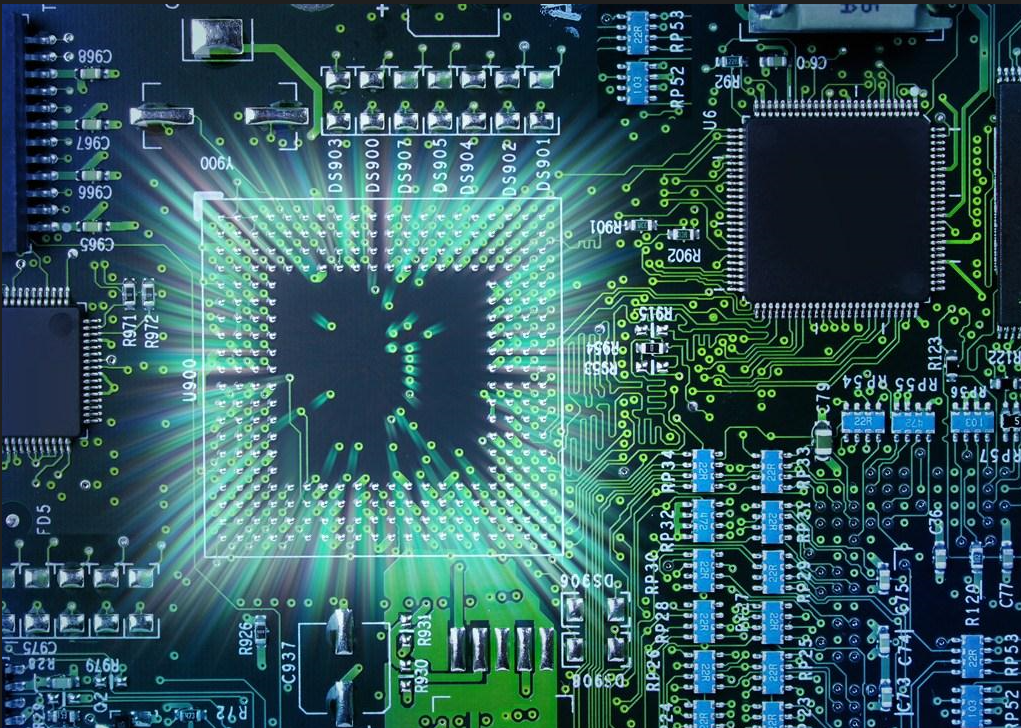
printed circuit board
Cause 2. The copper foil falls off from the PCB due to the customer. PCB design factors
1. PCB circuit design is unreasonable. If thick copper foil is used to design thin wires, the wires will be over matched and the copper foil will fall off.
Cause 3. PCB copper foil falls off PCB data
1. Ordinary electrolytic copper foil is galvanized or copper plated. If the peak value of the foil is abnormal during production or during galvanizing/copper plating, the coating crystal branch is poor, resulting in insufficient peel strength of the foil itself. When the bad foil is pressed into PCB, the copper wire will fall off under the impact of external force when it is inserted into the electronic equipment. This copper foil does not peel properly. The results show that there is no obvious side corrosion on the wool surface of the copper foil (i.e. the contact surface with the substrate), but the peel strength of the entire copper foil is poor.
2. Poor adaptability of copper foil to resin: Due to different resin systems, the curing agent used for some special PCBs, such as HTg board, is usually PN resin. The molecular chain structure of the resin is simple, and the crosslinking degree is low during curing. It is necessary to use special peak copper foil to match it. The copper foil used in the laminate production does not match the resin system, resulting in insufficient peeling strength of the metal foil coated with PCB and poor peeling of copper wires in the pieces.
The above is the explanation given by the editor of pcb circuit board company.
If you want to know more about PCBA, you can go to our company's home page to learn about it.
In addition, our company also sells various circuit boards,
High Frequency Circuit Board and SMT chip are waiting for your presence again.


抖音二維碼

Q Q二維碼

微信二維碼
點擊
然后
聯系
然后
聯系
電話熱線
13410863085Q Q

微信

- 郵箱