鑫景福致力于滿足“快速服務(wù),零缺陷,輔助研發(fā)”PCBA訂購單需求。


PCBA方案設(shè)計(jì)

The vision system makes PCB defects impossible to escape
In the world of modern electronIC products, printed circuit board is an important part of electronic products It is hard to imagine that any electronic equipment does not use PCB. In retrOSPect, the quality of PCB will have a significant impact on the long-term normal and reliable operation of electronic products Improving the quality of printed circuit board is an important problem that electronic product manufacturers should pay full attention to
If excessive or insufficient solder paste is SMEared on the bonding pad or no solder paste is placed at all during PCB assembly, the electronic connection between components and circuit board will be defective once solder joints are formed after subsequent reflow soldering. In fact, most defects can be found through the application of solder paste related quality traces.
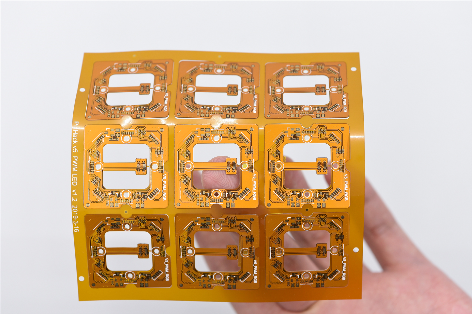
PCB board

At present, many circuit board manufacturers have adopted some online testing (ICT) or X-ray technology to detect the quality of solder joints. They will help eliminate defects in the printing process operation, but they cannot monitor the printing process operation itself. Misprinted circuit boards may experience additional process steps, and each step will add production costs to a certain extent, resulting in the final assembly stage of defective circuit boards. Manufacturers may have to discard defective boards or perform expensive and time-consuming repairs. At present, there may be no clear answer to the root cause of the defect.
Improper implementation of solder paste printing process may cause problems in electronic circuit connection. In order to effectively solve this problem, many screen printing equipment manufacturers have adopted online machine vision detection technology. Here is a brief introduction.
Online comprehensive visual inspection
More and more screen printing equipment manufacturers are incorporating online machine vision technology into their screen printing equipment to help Circuit board manufacturers detect defects in the early stages of their process implementation. The included vision system achieves three main goals:
First, they can detect defects directly after the printing operation is completed, allowing operators to deal with problems before adding major manufacturing costs to the circuit board. This is usually done after the cardboard is taken out of the printing unit, cleaned in the cleaning agent, repaired and returned to the production line.
Second, because defects are found at this stage, defective circuit boards can be prevented from reaching the back end of the production line. Therefore, it is necessary to prevent the repair phenomenon or the waste phenomenon formed in some occasions.
It may be important to inform the operator in a timely manner whether the printing process is running well, so as to effectively prevent defects.
In order to provide effective control in this level of process operation, an online vision system can be configured to detect the status of the bonding pad on the PCB after pasting, and whether the gap between the corresponding print templates is blocked or dragged. In most cases, components with SMAller spacing are tested to optimize test time and focus on problem areas. Remember, when possible problems are eliminated, the time spent on testing is very worthwhile.
CAMera positioning and detection
In traditional online visual inspection applications, the monitor is located above the circuit board to obtain the image of the printing position, and the relevant image can be sent to the processing system of the visual inspection equipment. There, the image analysis software compares the captured image with the reference image stored in the same location in the device memory.
Through this pipeline, the system can confirm whether too much or too little solder paste is used. The system also displays whether the solder paste is aligned on the pad. Can we find whether there is excess paste between the two pads, thus forming a bridge connection? This problem is also calLED "bridging" phenomenon by many PCB manufacturers.
The work of detecting the gap in the print template is completed in the same way. When excess solder paste accumulates on the printing plate surface, the vision system can be used to detect whether the gap is blocked by solder paste or whether there is tailing.
After the defects are found, the equipment can automatically request the following series of screen cleaning operations immediately, or rEMInd the operator of problems that need maintenance. Checking print templates can also provide users with very useful data about print quality and consistency.
One of the key functions of the online vision system is to detect PCB and pad surfaces with high reflectivity when the light is uneven or when the dry solder paste structure has an impact. For example, HASL boards are often uneven, with different surface profiles and reflection characteristics. Proper lighting also plays an important role in obtaining high-quality images.
The light must be able to "aim" at the reference and pad of the circuit board, so as to convert other fuzzy features into clear and recognizable shapes. The next step is to use VisionSoftwareAlgorithms to reach its full potential.
In some cases, the vision system can be used to detect the height or volume of solder paste on the pad, and sometiMES only the offline detection system can be used to detect. Using this program means that a corresponding degree of accumulation is formed in a given print template to confirm whether there is a lack of paste volume on the same plate.
Solder paste test
Specifically, it can be divided into two categories: detection of solder paste on PCB and detection of solder paste on printing template:
A. PCB detection
It mainly detects printing area, offset printing and bridging. The inspection of printing area refers to the solder paste area on each pad. Too much solder paste may lead to bridging, and too small solder paste may also lead to unstable solder joints. The printing offset is detected to check whether the paste amount on the printing plate is different from the specified position. The purpose of bridging test is to check whether the bonding amount between adjacent pads exceeds the specified amount. Excess solder paste may cause a short circuit.
B. Check printing template
Print template detection is mainly used for blocking and tracking. Jam detection refers to the detection of solder paste accumulation in the printing plate hole. If the hole is blocked, too little solder paste may be used at the next print point. Tailing detection refers to excessive solder paste accumulated on the surface of the printing template. Excess solder paste can be used in areas on the circuit board that should not be conductive, resulting in power connection problems.
Online machine vision systems can benefit PCB manufacturers with different pipes In addition to ensuring a high degree of solder joint integrity, it prevents manufacturers from wasting money on plate defects and the resulting rework Perhaps very important, it provides continuous process echo, which not only helps manufacturers optimize screen printing process, but also makes people more confident in this process
Causes and Solutions of PCB Heating
11-11,2022


抖音二維碼

Q Q二維碼

微信二維碼
點(diǎn)擊
然后
聯(lián)系
然后
聯(lián)系
電話熱線
13410863085Q Q

微信

- 郵箱