鑫景福致力于滿足“快速服務(wù),零缺陷,輔助研發(fā)”PCBA訂購單需求。


PCBA方案設(shè)計(jì)
Key factors affecting PCB manufacturability?
As an integral part of electronIC products, printed circuit boards (PCBs) play a key role in realizing the functions of electronic products This leads to PCB design, because PCB design directly determines the function of electronic products Expenses Outstanding PCB design can keep electronic products away from many problems, so as to ensure that the products can be successfully manufactured and meet all the needs of practical applications
PCB manufacturability
Because of the combination of manufacturability and PCB design, manufacturing design is the key element to achieve efficient manufacturing, high quality and low cost. The research scope of PCB manufacturability is very wide, which can be generally divided into PCB manufacturing and PCB assembly.
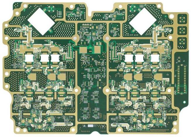
PCB production
For PCB manufacturing, the following aspects shall be considered: PCB size, PCB shape, process edge and MARKing point. Once these aspects are not fully considered in the PCB design stage, unless additional processing measures are taken, the automatIC chip placement machine may not be able to accept prefabricated PCB boards. To make matters worse, some circuit boards cannot be manufactured automatically by manual welding. In this case, the manufacturing cycle will be extended and the labor cost will be increased.
01. PCB size
Circuit board

Each mounter has its own required PCB size, which depends on the parameters of each mounter For example, the maximum PCB size accepted by the chip mounter is 500mm * 450mm, and the minimum PCB size is 30mm * 30mm This does not mean that we cannot handle the SMAller than 30mm * 30mm PCB components. When smaller sizes are needed, we can rely on jigsaw puzzles When only manual installation is required, labor costs rise, and the production cycle is out of control, the wafer placer will never accept too large or too small PCB boards Therefore, in the PCB design stage, the PCB size requirements for automatic installation and manufacturing settings must be fully considered and controlLED within the effective range
02, PCB shape
Except for PCB size, all wafer placers have requirements for PCB shape. Generally, the PCB shape should be rectangular, and the aspect ratio should be 4:3 or 5:4 (the best). If the shape of PCB is irregular, additional measures must be taken before SMT assembly, thus increasing the cost. In order to prevent this situation, PCB must be designed into a universal shape in the PCB design stage to meet the SMT requirements. However, it is difficult to do this in the actual situation. When the shape of some electronic products must be irregular, punch holes must be used to make the final PCB have a normal shape. After assembly, redundant auxiliary baffles can be omitted from the PCB to meet the requirements of automatic installation and space.
03, process side
In order to meet the needs of automatic manufacturing, the process edge must be placed on the PCB to fix the PCB.
In PCB design stage, 5mm wide process edge shall be reserved in advance without any components and traces. The science and technology guide is usually placed on the short side of PCB, but when the aspect ratio exceeds 80%, the short side can be selected. After assembly, the process side used as an auxiliary production role can be disassembled.
04 Reference point (marking point)
For PCB with components installed, mark points should be added as common reference points to ensure that each assembly device can accurately determine the position of components. This mark point is the SMT manufacturing benchmark required for automatic manufacturing.
Components require 2 marker points, while PCB requires 3 marker points. These marks should be placed on the edge of the PCB and cover all SMT components. The center distance between the marking point and the edge of the circuit board shall be at least 5 mm. For PCB with double-sided SMT components, there should be marked points on both sides. If components are placed too densely to place marker points on the circuit board, they can be placed on the process edge.
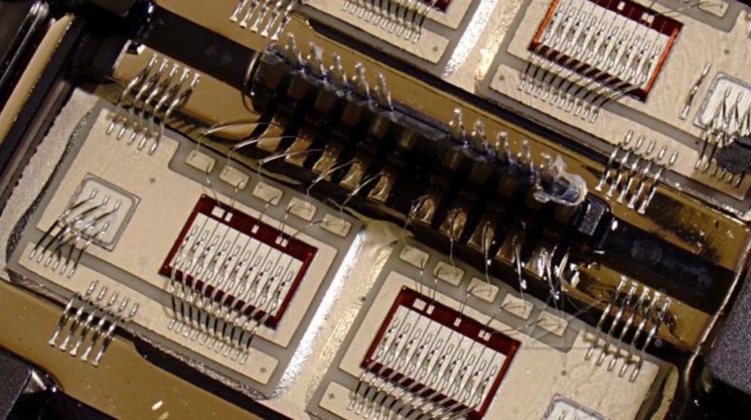
PCB assembly
PCB assembly, or PCBA for short, is actually the process of welding components on bare boards. In order to meet the requirements of automatic manufacturing, PCB assembly puts forward some requirements for component packaging and component layout.
01. Component packaging
During PCBA Design, if the packaging of components does not meet the appropriate standards and the distance between components is too close, automatic installation will not be performed.
In order to obtain the best component packaging, professional EDA design software compatible with international component packaging standards should be used. During PCB design, the aerial view area shall not overlap with other areas, and the automatic IC placement machine will be able to accurately identify and surface mount.
02, Layout of components
Component layout is an important task in PCB design, because its effectiveness is directly related to the appearance of PCB and the complexity of manufacturing process.
During component layout, the assembly surfaces of SMD components and THD components shall be determined. Here, the front side of the PCB is set as the component A side, and the back side is set as the component B side. Assembly form shall be considered for component layout, including single-layer single package component, double-layer single package component, single-layer hybrid package component, A-side hybrid package and B-side single package component, and A-side THD and B-side SMD components. Different assemblies require different manufacturing technologies and technologies. In terms of component layout, the best component layout shall be selected to make manufacturing SIMple and easy, so as to improve the manufacturing efficiency of the whole process.
In addition, the direction of component layout, spacing between components, heat dissipation and component height must be considered.
In general, the component orientation should be consistent. The component layout complies with the principle of shortest tracking distance. According to this principle, the polarity direction of the components with polarity marks shall be consistent, and the components without polarity marks shall be neatly arranged on the X or Y axis. The height of the element shall not exceed 4mm, and the transmission direction of the element and PCB shall be kept at 90 °.
In order to improve the welding speed of components and facilitate later inspection, the spacing between components shall be consistent. Elements in the same network shall be close to each other, and safe distance shall be kept between different networks according to voltage drop. The wire MESh and cushion shall not overlap, otherwise the components will not be installed.
Due to PCB design and thermal characteristics of power components, heat dissipation should be considered The layout of components shall pay attention to heat dissipation, and fans or radiators shall be used when necessary Proper radiator shall be selected for power components, and thermal sensor shall be far away from heat source The high assembly shall be placed behind the low assembly


抖音二維碼

Q Q二維碼

微信二維碼
點(diǎn)擊
然后
聯(lián)系
然后
聯(lián)系
電話熱線
13410863085Q Q

微信

- 郵箱