鑫景福致力于滿足“快速服務(wù),零缺陷,輔助研發(fā)”PCBA訂購單需求。


PCBA方案設(shè)計
About the differences of multilayer circuit boards
printed circuit board, that is, printed circuit board, is not only the support of electronIC components, but also the carrier of electrICal connection of electronic components In the printed circuit board (PCB), the connection between electronic components is completed through direct connection of wires; But now, wiring methods are only used for laboratory tests, and printed circuit boards occupy an absolute control position in the electronic industry
The Past and Present of PCB
The development history of printed circuit board can be traced back to the early 20th century. In 1936, Paul Eisler, an Austrian, applied the printed circuit board to the radio and put it into practical use for the first time; In 1943, the United States widely used this technology in military radios; In 1948, the United States officially recognized that the invention could be used for commercial purposes. Since the mid 1950s, printed circuit boards have been widely used and entered a period of rapid development.
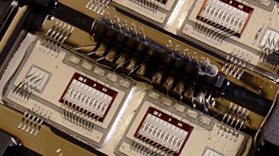
Explore the Mystery of Multilayer Circuit Board
As PCB becomes more and more complex, when designers use development tools to design PCB, it is easy to confuse the definition and purpose of each layer. When our hardware developers Draw PCB by themselves, it is easy to cause unnecessary misunderstanding in production, because they are not familiar with the use of each layer of PCB. To avoid this situation, take AltiumDesignerSummer09 as an example to classify and introduce each PCB layer.
Printed circuit board

Differences between PCB layers (signal layer)
AltiumDesigner can provide up to 32 signal layers, including the top layer (top layer), bottom layer (bottom layer) and middle layer (middle layer). These layers can be interconnected by via, BlindVia, and BuriedVia.
Explore the Mystery of multilayer circuit board
1. Top signal floor (top floor)
Also calLED component layer, it is mainly used to place components. For double-layer boards and multilayer boards, it can be used to arrange wires or copper.
2. Ground floor
Also called welding layer, it is mainly used for wiring and welding of printed circuit board It can be used to place components of double-layer and multilayer plates
3. Middle layer
Up to 30 layers can be used to arrange signal lines in Multilayer boards. Power cord and ground wire are not included here.
Internal Planes
Usually referred to as the inner electric layer, it only appears in multilayer boards. The number of PCB layers usually refers to the sum of signal layer and internal electrical layer. Like the signal layer, the inner electric layer and the inner electric layer can be connected with each other through through holes, blind holes and buried holes.
Explore the Mystery of Multilayer Circuit Board
Screen fabric
A printed circuit board can have at most two silk screen layers, namely the top silk screen layer and the bottom silk screen layer, which are usually white. They are mainly used to place printing information, such as component outlines and notes, various note characters, etc., to facilitate the welding of components of the printed circuit board and circuit inspection.
1. Top Overlay
It is used to MARK the projection outline of the part, label, nominal value or model of the part, and various comment characters.
2. Bottom cover
Same as the top screen layer. If all the marks on the top screen layer are included, the bottom screen layer can be closed.
Mechanical layer (mechanical layer)
The mechanical layer is usually used to place instruction information about the manufacturing and assembly methods of circuit boards, such as the overall dimensions, dimension marks, data data, through-hole information, assembly instructions and other information of printed circuit boards. This information varies according to the requirements of the design company or printed circuit board manufacturer. The following example illustrates our common approach.
1: Usually used to draw the frame of a printed circuit board as its mechanical shape, this is also called a shape layer;
2: We are used to placing PCB processing process requirements table, including size and other information, plates, layers, etc;
Body size information of most parts in ETM database, including 3D models of parts; To SIMplify the page, this layer is not displayed by default;
The package information of most components in the ETM library can be used to estimate the size of PCB at the early stage of the project; To simplify the page, this layer is not displayed by default, and the color is black.
MaskLayers
Altium Designer provides two types of mask layers (SolderMask) and PasteMask, including two layers, the top layer and the bottom layer.

Quality Control in PCBA and SMT Production
11-17,2022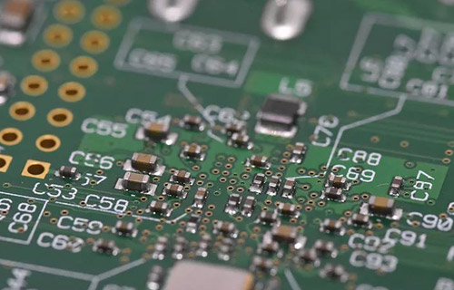


抖音二維碼

Q Q二維碼

微信二維碼
點(diǎn)擊
然后
聯(lián)系
然后
聯(lián)系
電話熱線
13410863085Q Q

微信

- 郵箱