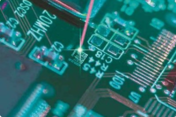
鑫景福致力于滿足“快速服務,零缺陷,輔助研發”PCBA訂購單需求。


PCBA方案設計
The practICal dry goods of PCB design reliability design specification mainly introduces that electronIC design engineers should remember and practice the most effective reliability design rules when using design software for PCB layout design and commercial manufacturing.
1. PCB wiring and layout isolation criteria: strong and weak current isolation, large and SMAll voltage isolation, high and low frequency isolation, input and output isolation, digital analog isolation, input and output isolation. The dividing standard is one order of magnitude difference. The isolation methods include space separation and ground wire separation.

2. Wiring of crystal oscillator in PCB design: the crystal oscillator shall be close to the IC as much as possible, and the wiring shall be thick, and the shell of crystal oscillator shall be grounded.
3. When the clock wiring is output through the connector, the pins on the connector shall be covered with grounding pins around the clock wire pins.
4. Let analog and digital circuits have their own power supply and ground wire paths. If possible, widen the power supply and ground wire of these two parts of circuits or use separate power supply layer and ground plane to reduce the impedance of power supply and ground wire circuits and reduce any possible interference voltage in power supply and ground wire circuits.
5. The analog ground and digital ground of PCBs that work independently can be connected at a single point near the system grounding point. If the power supply voltage is consistent, the power supplies of analog and digital circuits can be connected at a single point at the power supply inlet. If the power supply voltage is inconsistent, a 1~2nf capacitor near the two power supplies can provide a path for the signal return current between the two power supplies.
6. If the PCB is inserted on the motherboard, the power and ground of the analog and digital circuits of the motherboard should also be separated. The analog ground and digital ground should be grounded at the grounding point of the motherboard, and the power supply should be connected at a single point near the system grounding point. If the power supply voltage is consistent, the power supplies of the analog and digital circuits should be connected at a single point at the power supply inlet. If the power supply voltage is inconsistent, a 1~2nf capacitor should be connected at the close place of the two power supplies, Provide a path for the signal return current between the two power supplies.
7. When high-speed, medium speed and low-speed digital circuits are mixed, different layout areas should be assigned to them on the PCB.
8. Low level analog circuit and digital logic circuit shall be separated as far as possible.
9. In the design of multilayer printed boards, the power plane shall be close to the grounding plane and arranged below the grounding plane and adjacent to the entire metal plane.
10. The digital circuit and analog circuit shall be separated in the design of multilayer printed circuit board, and the digital circuit and analog circuit shall be arranged in different layers when conditions permit. If it must be arranged on the same floor, it can be remedied by trenching, adding grounding lines, separation and other methods. The analog and digital ground and power supplies shall be separated and cannot be mixed.
PCB design wiring and layout PCB layout
PCB design wiring and layout - PCB layout. Here are a few SIMple points about PCB design wiring and layout. We will continue to update and learn more in the future.
1. Clock circuit and high-frequency circuit are the main interference and radiation sources, which must be arranged separately and away from sensitive circuits
2. Pay attention to waveform distortion during long line transmission
3. The best way to reduce the loop area of interference sources and sensitive circuits is to use twisted pairs and shielded wires to twist the signal wire and the grounding wire (or current carrying loop) together, so that the distance between the signal and the grounding wire (or current carrying loop) is the shortest
4. Increase the distance between lines, so that the mutual inductance between the interference source and the induced line is as small as possible. If possible, the interference source line and the induced line are arranged at right angles (or close to right angles), which can greatly reduce the coupling between the two lines
5. Increasing the distance between lines is the best way to reduce capacitive coupling
6. Before formal wiring, the first thing is to classify the lines. The main classification method is based on power level, which is divided into several groups for each 30dB power level
7. Wires of different classifications shall be bundLED and laid separately. The adjacent conductors can also be grouped together after shielding or twisting. The minimum distance between harnesses laid by category is 50~75mm
8. When arranging the resistance, the gain control resistor and bias resistor (up and down) of the amplifier, pull-up and voltage stabilizing rectifier circuit should be as close to the amplifier, active devices and their power supply and ground as possible to reduce their decoupling effect (improve the transient response time).
9. The bypass capacitor is placed close to the power input, and the decoupling capacitor is placed at the power input.
10. As close to each IC as possible
11. Basic characteristic impedance of PCB: determined by the quality of copper and cross section area. Specifically: 1 oz 0.49 mOhm/unit area.
Capacitance: C=EoErA/h, Eo: permittivity of free space, Er: permittivity of PCB substrate, A: range of current, h: line spacing
Inductance: It is evenly distributed in the wiring, about 1nH/moz copper wire. Under the rolling of 0.25mm (10mil) thick FR4, 0.5mm wide and 20mm long wire above the ground layer can produce 9.8 milliohms of impedance, 20nH inductance and 1.66pF coupling capacitance with the ground.
12. Basic principle of PCB wiring: increase wiring spacing to reduce capacitance coupling crosstalk; Lay the power line and ground wire in parallel to optimize PCB capacitance; The sensitive high-frequency line shall be arranged far away from the high noise power line; Widen the power line and ground wire to reduce the impedance of the power line and ground wire.
13. Division: use physical division to reduce the coupling between different types of signal lines, especially the power supply and ground wire.
14. Local decoupling: decouple the local power supply and IC, use large capacity bypass capacitors between the power input port and PCB for low-frequency ripple filtering and meet the requirements of sudden power, use decoupling capacitors between the power supply and ground of each IC, and these decoupling capacitors should be as close to the lead pin as possible.
15. Wiring separation: minimize crosstalk and noise coupling between adjacent lines in the same PCB layer. The 3W specification is used to process key signal paths.
16. Protection and shunt circuit: the key signals shall be protected by two ground wires, and both ends of the protection circuit shall be grounded.


抖音二維碼

Q Q二維碼

微信二維碼
點擊
然后
聯系
然后
聯系
電話熱線
13410863085Q Q

微信

- 郵箱