鑫景福致力于滿足“快速服務,零缺陷,輔助研發”PCBA訂購單需求。


PCBA方案設計
PCB design (Printed Circuit Board Design): based on the circuit schematIC diagram, realize the functions required by the circuit designer.
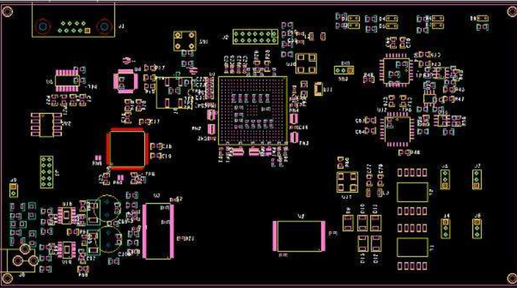
The design of printed circuit board mainly refers to layout design, which needs to consider the layout of external connections. Optimized layout of internal electronIC components. Optimized layout of metal wiring and through-hole. Electromagnetic protection. Heat dissipation and other factors.
Excellent layout design can save production costs and achieve good circuit performance and heat dissipation. SIMple layout design can be realized by hand, while complex layout design needs to be realized by computer aided design (CAD).

PCB design steps:
I. Layout design
In PCB, special components refer to the key components in the high-frequency part, the core components in the circuit, the components susceptible to interference, the components with high voltage, the components with high heat, and some heterosexual components. The positions of these special components need to be carefully analyzed, and the tape layout should meet the requirements of circuit functions and Production requirements. Improper placement of them may cause circuit compatibility problems and signal integrity problems, which may lead to PCB design failure.
The PCB size shall be considered first when placing special components in the design. Quick buy points out that when PCB size is too large, the printing line is long, the impedance increases, the dry resistance decreases, and the cost increases; If it is too SMAll, the heat dissipation is poor, and adjacent lines are easily disturbed. After determining the size of PCB, determine the swing position of special components. Finally, all components of the circuit are arranged according to the functional unit. The location of special components shall generally comply with the following principles:
1. Shorten the connection between high-frequency components as much as possible, and try to reduce their distribution parameters and mutual electromagnetic interference. Components susceptible to interference shall not be too close to each other, and the input and output shall be as far away as possible.
2 Some components or wires may have high potential difference, so their distance shall be increased to avoid accidental short circuit caused by discharge. High voltage components should be kept out of reach.
3. Components weighing more than 15G can be fixed with brackets and then welded. Those heavy and hot components should not be placed on the circuit board, but on the bottom plate of the main box, and heat dissipation should be considered. Thermal components shall be far away from heating components.
4. For the layout of adjustable components such as potentiometers, adjustable inductance coils, variable capacitors, microswitches, etc., the structural requirements of the whole wrench should be considered. Some switches that are often used should be placed in places that are easy to reach when the structure allows. The Layout of components should be balanced, and the density should be appropriate.
For the success of a product, the first is to pay attention to the internal quality. It is necessary to give consideration to the overall beauty. Only the perfect wrench of both can become a successful product.
II. Placing sequence
1. Place components closely matching with the structure, such as power socket, indicator light, switch, connector, etc.
2. Place special components, such as large components, heavy components, heating components, transformers, ICs, etc.
3. Place small components.
III. Layout inspection
1. Whether the size of PCB is consistent with the processing size required by the drawing.
2. Whether the layout of PCB components is balanced, orderly arranged and completely distributed.
3. Whether there are conflicts at all levels. Such as whether the components, fraMES, and layers requiring private printing are reasonable.
3. Whether the commonly used components are convenient for use. Such as switches, plug-in devices, components that must be replaced frequently, etc.
4. Whether the distance between thermal components and heating components is reasonable.
5. Whether the heat dissipation is good.
6. Whether the interference of the line needs to be considered.
PCB design skills:
I. Setting Skills
Different point settings are required in different stages of the design, and large grid points can be used for device layout in the layout stage;
For large devices such as IC and non positioning connector, the grid point accuracy of 50-100 mil can be selected for layout, while for passive small devices such as resistance, capacitance and inductance, the grid point of 25 mil can be used for layout. The accuracy of large grid points is conducive to the alignment and beautiful layout of devices.
PCB layout rules:
1. In general, all components should be arranged on the same side of the circuit board. Only when the top layer components are too dense can some devices with limited height and low heat generation, such as chip resistance, chip capacitance, chip IC, etc., be placed on the bottom layer.
2. On the prEMIse of ensuring the electrical performance, the elements shall be placed on the grid and arranged in parallel or vertical to each other for neat and beautiful appearance. In general, the elements are not allowed to overlap; The elements shall be arranged compactly, and the elements shall be evenly distributed and uniformly spaced throughout the layout.
3. The minimum spacing between adjacent pad patterns of different components on the circuit board shall be more than 1MM.
4. The distance from the edge of the circuit board is generally not less than 2 mm. The best shape of the circuit board is rectangular, with a length to width ratio of 3:2 or 4:3. When the size of the circuit board is greater than 200 mm by 150 mm, the mechanical strength that the circuit board can withstand should be considered.
II. PCB Layout Skills
In the layout design of PCB, the unit of the circuit board shall be analyzed, and the layout design shall be carried out according to the function. The layout of all components of the circuit shall comply with the following principles:
1. Arrange the position of each functional circuit unit according to the circuit flow, so that the layout is convenient for signal flow and the signal is kept in the same direction as far as possible.
2. The layout is centered on the core components of each functional unit. The components and parts shall be evenly, integrally and compactly arranged on the PCB to minimize and shorten the leads and connections between components and parts.
3. For circuits operating at high frequencies, the distribution parameters between components should be considered. In general, components shall be arranged in parallel as far as possible, which is not only beautiful, but also easy to assemble and weld, and easy to mass produce.
The above is the introduction of PCB design and the general content of the steps. To become a real PCB design expert, you still need more practice!


抖音二維碼

Q Q二維碼

微信二維碼
點擊
然后
聯系
然后
聯系
電話熱線
13410863085Q Q

微信

- 郵箱