鑫景福致力于滿足“快速服務(wù),零缺陷,輔助研發(fā)”PCBA訂購單需求。


PCBA方案設(shè)計
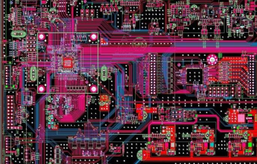
NovICe often do not understand some rules of PCB layout in PCB design, which often leads to serious production accidents in the designed PCB. Here are some common rules of PCB layout design.
1. Even though the power supply and ground wire are handLED so well that the wiring in the entire PCB board is completed, the interference caused by improper consideration of the power supply and ground wire will degrade the performance of the product, and sometiMES even affect the success rate of the product. Therefore, the wiring of electrical and ground wires should be taken seriously to minimize the noise interference generated by electrical and ground wires to ensure the quality of products.

2. Common ground processing of digital circuits and analog circuits Now many PCBs are no longer single functional circuits (digital or analog circuits), but composed of digital circuits and analog circuits. Therefore, when wiring, it is necessary to consider the mutual interference between them, especially the noise interference on the ground wire. The frequency of digital circuit is high and the sensitivity of analog circuit is strong. For the signal line, the high-frequency signal line is as far away from the sensitive analog circuit device as possible. For the ground wire, the integrated PCB has only one node to the outside world. Therefore, the problem of digital and analog common ground must be handled inside the PCB. In fact, the digital ground and analog ground inside the board are not connected with each other, Only at the interface between PCB and the outside world (such as plug). There is a short circuit between digital ground and analog ground. Please note that there is only one connection point. Some are not common on PCB, which is determined by system design.
3. When the signal line is laid on the electrical (ground) layer and on the multilayer printed circuit board, there are not many lines left in the signal line layer. The additional layers will cause waste and increase the workload and cost of production. In order to solve this contradiction, wiring on the electrical (ground) layer can be considered. The power layer should be considered first, and then the stratum. Because it is better to preserve the integrity of the stratum.
4. Treatment of connecting legs in large-area conductors In large-area grounding (electricity), the legs of commonly used components are connected with them, and the treatment of connecting legs needs to be considered comprehensively. As far as electrical performance is concerned, it is better to fully connect the bonding pad of component legs with the copper surface, but there are some hidden dangers in the welding assembly of components, such as: ① Welding requires high-power heaters. ② It is easy to cause false solder joints. Therefore, taking into account the electrical performance and process needs, a cruciform pad is made, which is called heat shield, commonly known as thermal pad. In this way, the possibility of false solder joints due to excessive heat dissipation of the section during welding can be greatly reduced. The treatment of the electric (grounding) leg of the Multilayer board is the same.
5. The role of network system in cabling is in many CAD systems, and cabling is determined by the network system. The grid is too dense, the access is increased, but the step size is too SMAll, and the amount of data in the map field is too large, which inevitably requires higher storage space of the equipment, and has a great impact on the operation speed of computer electronic products. However, some channels are invalid, such as those occupied by the pad of the component leg or by the mounting hole or the fixing hole. Too sparse grid and too few paths have a great impact on the deployment rate. Therefore, it is necessary to have a reasonably dense grid system to support the routing. The distance between the legs of standard components is 0.1 inch (2.54mm), so the foundation of the grid system is generally 0.1 inch (2.54 mm) or an integral multiple of less than 0.1 inch, such as 0.05 inch, 0.025 inch, 0.02 inch, etc.
6. Design Rule Check (DRC) After the wiring design is completed, it is necessary to carefully check whether the wiring design conforms to the rules formulated by the designer, and also to confirm whether the rules formulated conform to the requirements of the PCB production process. Generally, the inspection includes the following aspects: line to line, line to component pad, line to through hole, component pad to through hole, and the distance between through hole and through hole is reasonable, Whether the Production requirements are met.
2. Design process: PCB design process is divided into six steps: netlist input, rule setting, component layout, wiring, inspection, recheck, and output
2.1 Netlist input There are two methods for netlist input. One is to use the OLE PowerPCB Connection function of PowerLogic, select Send Netlist, and use the OLE function to keep the schematic and PCB diagrams consistent at any time, so as to minimize the possibility of errors. The other method is to directly load the netlist in PowerPCB, select File ->Import, and input the netlist generated by the schematic diagram.
2.2 Rule Setting If the PCB design rules have been set in the schematIC design stage, you do not need to set these rules, because when you input the net list, the design rules have been entered into PowerPCB along with the net list. If the design rules are modified, the schematic diagram must be synchronized to ensure the consistency between the schematic diagram and PCB. In addition to the design rules and layer definitions, there are also some rules that need to be set, such as Pad Stacks, and the size of standard vias needs to be modified. If the designer creates a new pad or via, be sure to add Layer 25.
2.3 After the component layout netlist is input, all components will be placed at the zero point of the work area and overlapped. The next step is to separate these components and place them neatly according to some rules, that is, component layout. PowerPCB provides two methods, manual layout and automatic layout.
2.3.1 Manual layout 1. Draw the board outline for the structural size of the tool printed board. 2. Disperse components, and components will be arranged around the board edge. 3. Move and rotate the components one by one, place them inside the board edge, and place them neatly according to certain rules.
2.3.2 Automatic Layout PowerPCB provides automatic layout and automatic local cluster layout, but for most designs, the effect is not ideal, so it is not recommended.
2.3.3 Precautions
a. The primary principle of layout is to ensure the distribution rate of wiring, pay attention to the connection of flying wires when moving components, and put the components with wiring relationship together
b. Digital devices and analog devices shall be separated and kept as far away as possible
c. The decoupling capacitor shall be as close to the VCC of the device as possible
d. When placing the device, consider the future welding, not too intensive
e. Use the Array and Union functions provided by the software to improve the layout efficiency
2.4 There are also two ways of wiring, manual wiring and automatic wiring. PowerPCB provides powerful manual routing functions, including automatic crowding and online design rule checking (DRC). Automatic routing is performed by Specctra's routing engine. Usually, the two methods are used together. The common steps are manual automatic manual.
2.4.1 Manual wiring
1. Before automatic wiring, some important networks, such as high-frequency clock, main power supply, etc., should be manually distributed. These networks often have special requirements for routing distance, line width, line spacing, shielding, etc; In addition, for some special packages, such as BGA, automatic wiring is difficult to arrange in a regular way, and manual wiring is also required. 2. After automatic wiring, manual wiring should also be used to adjust PCB wiring.
2.4.2 After the automatic wiring and manual wiring are completed, the rest of the network will be handed over to the automatic router. Select Tools ->SPECCTRA, start the interface of the Specctra router, set the DO file, and press Continue to start the automatic routing of the Specctra router. After that, if the routing rate is 100%, you can manually adjust the routing; If it is less than 100%, it indicates that there is a problem with the layout or manual wiring, and it is necessary to adjust the layout or manual wiring until all wiring is completed.
2.4.3 Precautions
a. Power line and ground wire shall be thickened as much as possible
b. Decoupling capacitor shall be directly connected with VCC as far as possible
c. When setting the DO file of Specctra, first add the Protect all wires command to protect the manually laid wires from being re laid by the automatic router
d. If there is a hybrid power layer, it should be defined as Split/Mixed Plane. Before wiring, it should be divided. After wiring, use the Plane Connect of Pour Manager for copper coating
e. Set all device pins to the hot pad mode by setting Filter to Pins, selecting all pins, modifying the attributes, and checking f in front of the Thermal option. Open the DRC option during manual wiring, and use Dynamic Route
2.5 The items to be checked include Clearance, Connectivity, High Speed and Plane. Tools>Verify Design can be selected for these items. If the high-speed rule is set, it must be checked, otherwise this item can be skipped. Errors are detected and the layout and routing must be modified. Note: Some errors can be ignored. For example, some parts of the Outline of some connectors are placed outside the board frame, and errors will occur when checking the spacing; In addition, every time the routing and vias are modified, they should be copper coated again.
2.6 Recheck According to the "PCB checklist", the contents include design rules, layer definition, line width, spacing, pad and via settings; The rationality of device layout, the routing of power supply and ground network, the routing and shielding of high-speed clock network, and the placement and connection of decoupling capacitors should also be reviewed. If the recheck is unqualified, the designer shall modify the layout and wiring. After the recheck is qualified, the reviewer and the designer shall sign respectively.
2.7 Design Output PCB design can be output to a printer or photo file. The printer can print PCB layer by layer, which is convenient for designers and reviewers to check; The photo drawing documents shall be submitted to the board manufacturer for the production of printed boards. The output of photo files is very important, which is related to the success or failure of this design. The following will focus on the precautions for outputting photo files.
a. The layers to be output include wiring layer (including top layer, bottom layer and intermediate wiring layer), power layer (including VCC layer and GND layer), silk screen layer (including top layer silk screen and bottom layer silk screen), solder mask layer (including top layer solder mask and bottom layer solder mask), and also generate drilling file (NC Drill)
b. If the power supply layer is set to Split/Mixed, select Routing in the Document item of the Add Document window, and use the Plane Connect of Pour Manager to copper-clad PCB drawings before outputting photo files each time; If it is set to CAM Plane, select Plane. When setting Layer, add Layer25, and select Pads and Viasc in Layer25 In the device setup window (press Device Setup), change the Aperture value to 199
d. When setting the Layer of each layer, select Board Outline
e. When setting the layer of the silk screen layer, do not select the Part Type, but select the Outline, Text and Line of the top (bottom) and silk screen layer
f. When setting the layer of solder mask layer, selecting via means no solder mask is added to the via, and not selecting via means home solder mask, depending on the specific situation
g. When generating the drilling file, use the default settings of PowerPCB and do not make any changes
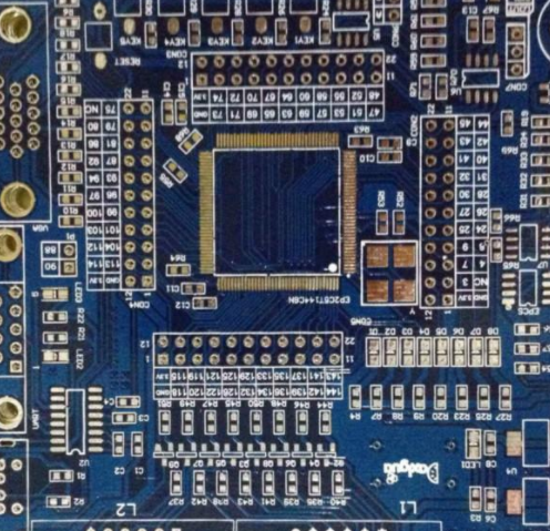
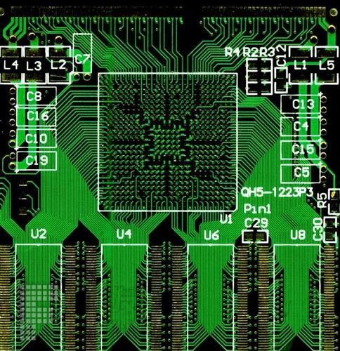
h. After all photo files are output, open them with CAM350 and print them. The designer and reviewer check vias (via) according to the "PCB checklist", which is one of the important components of multilayer PCBs. The cost of drilling usually accounts for 30% to 40% of the cost of PCB making.
2、 Parasitic capacitance of via The via itself has parasitic capacitance to ground. If it is known that the diameter of the isolation hole of the via on the floor is D2, the diameter of the via pad is D1, the thickness of the PCB is T, and the dielectric constant of the board substrate is ε, Then the parasitic capacitance of the via is approximately C=1.41 ε The parasitic capacitance of TD1/(D2-D1) via will mainly affect the circuit by prolonging the signal rise time and reducing the circuit speed. For example, for a PCB with a thickness of 50Mil, if a via with an inner diameter of 10Mil and a pad diameter of 20Mil is used and the distance between the pad and the ground copper area is 32Mil, we can approximately calculate the parasitic capacitance of the via through the above formula: C=1.41x4.4 x 0.050 x 0.020/(0.032-0.020)=0.517pF, and the rise time change caused by this part of capacitance is T10-90=2.2C (Z0/2)=2.2 x 0.517x (55/2)=31.28ps. It can be seen from these values that, although the effect of the rise delay caused by the parasitic capacitance of a single via is not obvious, the designer should carefully consider if the via is used for switching between layers for many times in routing.


抖音二維碼

Q Q二維碼

微信二維碼
點(diǎn)擊
然后
聯(lián)系
然后
聯(lián)系
電話熱線
13410863085Q Q

微信

- 郵箱