鑫景福致力于滿足“快速服務,零缺陷,輔助研發”PCBA訂購單需求。


PCBA方案設計
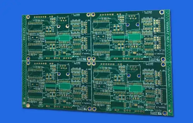
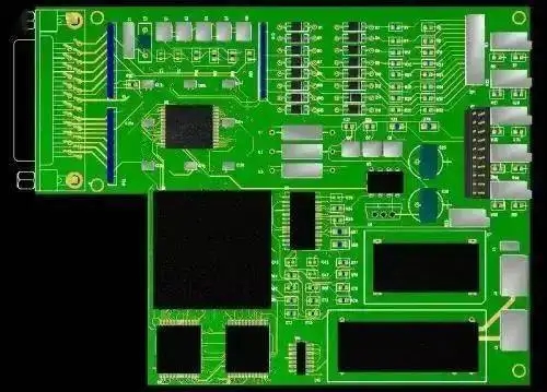
PCB manufacturers offer you PCB layout and wiring skills Q 4
Now, although there are many software that can realize PCB automatIC layout and routing. However, as the signal frequency continues to increase, in many cases, engineers need to understand the basic principles and skills of PCB layout and wiring to make their design perfect.
76. Question: In DC-DCConvertetIC, you need to connect to the ground plane below the IC, and connect to the ground plane through Via. What is the impact of the number of Via holes?
Answer: Generally, it can be designed according to the reference design. Due to the large current, a certain amount of Via may be required.
77. Question: During impedance matching, if the impedance value given by the pin is complex, that is, there is both impedance and reactance, how to do impedance matching? Is the resistance part considered?
Answer: Consider conjugate matching to cancel the imaginary part of impedance.
78. Question: Which is better, the concentrated parameter or the distributed parameter in high frequency? How to choose these two methods?
A: The distribution method is relatively high, but complex; The aggregation method is relatively SIMple, but there are some errors.
79. Question: What are the requirements for the distribution of vias connecting the upper and lower copper clad floors of the double-layer board?
A: Generally speaking, there should not be too many requirements for separation if it is only to improve connectivity.
80. Q: How to balance the parasitic inductance and capacitance of the amplifier input in IF applications?
Answer: Generally speaking, the influence of parasitic inductance and capacitance on IF circuit is SMAll and can be ignored. As long as it is ensured that large parasitic capacitance and inductance values are not introduced.
81. Q: How can the interference between circuit components be effectively reduced, and how can the amplifier layout limit the introduction of ripple?
Answer: The principle of reducing interference is:
Reduce radiation end;
Strengthen the interference isolation, shielding and decoupling;
The principle of ripple reduction is also:
Reduce ripple output of switching power supply;
Sufficient decoupling filtering;
82. Question: In the 6-tier design, what are the layer allocation skills and which routing needs to go through the middle tier?
A: It depends on your design. The principle is to ensure that there are two separate layers of analog signal line and analog ground.
83. Question: When connecting analog ground and digital ground, is the method adopted to connect a suitable magnetic bead to the analog ground at the digital ground? How to choose this magnetic bead?
Answer: Magnetic beads are mainly used to isolate high-frequency noise. Different magnetic beads have different filtering frequencies, so appropriate devices should be selected according to the noise on the board.
84. Q: What should I pay attention to for the signal layout above 5G?
A: Transmission line effect, parasitic effect and EMI should be considered.
85. Question: When there are high-speed logic devices in the circuit, what is the wiring length?
Answer: Wiring is not afraid of length, but of asymmetry or large difference, which is easy to cause wrong logic due to delay.
86. Question: In high-speed digital circuit boards, there are multiple power supplies with different voltage values. When laying the power supply plane, should we try to use multi-layer power supply planes or separate them on the same power supply plane?
Answer: Multiple voltages can be applied on one plane. Pay attention to the isolation between them. It is also possible to separate the important power supply, so as to ensure that it is not interfered by other power supplies.
87. Question: Due to space constraints, the differential line cannot be fully equidistant and equal length. Would you like to ask whether to give priority to equidistance or equal length?
Answer: Equal length can ensure impedance matching, but unequal distance actually has an impact on differential matching, which requires simulation testing.
88. Q: How to reduce EMI in PCB layout? Which other modules should be closer to the main control chip?
Answer: The main controller mainly transmits digital signals, so the analog and power parts should be far away from the controller; For reducing electromagnetic interference, it is necessary to pay attention to matching, decoupling, layout, layering and other issues. It is recommended to refer to some information.
89. Question: When considering signal integrity, if we only know that the frequency of the digital chip is 1GHz, we will generally estimate that its rise time is 1/10 of the cycle, that is, 0.1ns. Is there any basis?
Answer: This is a general principle. The speed of the edge depends on the speed of the device output port. If it is too slow, it will affect the judgment. Soon, the chip process can not reach.
90. Q: Hello, ARM chip can improve the anti-interference of power supply. In addition to connecting TVS tube at the power input end, is it better to connect the input pin of power input end with inductance or magnetic bead?
Answer: Generally, magnetic beads are used.
91. Question: Can the PCB board be simulated online, that is, how to verify whether there is a problem with the lower board?
Answer: Some PCB software can do some wiring inspection and integrity analysis, such as CADence.
92. Question: When wiring the pcb, some people connect a resistor in series at the input and output terminals of the signal. Does this play a big role? How to select this resistor? Where does this need to be done?
Answer: It depends on the effect of series resistance. Some of them play the role of current limiting, and some may do impedance matching.
93. Q: Are there any good suppression scheMES or relatively systematic processing methods for high-speed pulse trains that affect the power supply?
Answer: Your so-calLED high-speed pulse train is nothing more than interference signals of different frequencies, which use capacitance decoupling of different values.
94. Question: Are there any special requirements for high-speed PCB boards?
Answer: High frequency circuit has requirements for PCB materials. Transmission line effect should be considered at high frequency.
95. Question: Please introduce and practice the impedance matching of signal lines?
Answer: In case of low frequency, it is necessary to consider the relationship between the width of the signal line and the current carrying capacity. In case of high frequency, it is necessary to consider matching equal length and other issues.
96. Q: What are the anti-interference measures for high-frequency signal lines? What should I pay attention to when wiring?
A: This question is rather broad, and it is difficult to make it clear in one or two sentences.
97. Q: Why do high-speed signals not have to be divided into digital and analog signals?
Answer: Because the driver side can adjust the output phase difference, it is difficult to adjust after the PCB layout is completed. The receiver side inputs directly and cannot adjust.
98. Question: Why do you directly suggest compensation at the driver side for equal length compensation of differential line? Can you explain it? Eric Bogatin only gives conclusions in his book, but there is no explanation.
Answer: Some chips at the driver end have the adjustment function. The PCB line design has not been easily changed. Generally, the direct input at the receiver end does not have the function of time delay adjustment.
99. Question: Is the dielectric constant as small as possible when selecting plate materials at high frequencies?
Answer: It means that the parasitic capacitance is small. However, the design of the characteristic impedance of the signal line requires the dielectric constant, which cannot be generalized.
100. Question: What frequency of crystal oscillator should consider the wiring mode between MCU and crystal oscillator?
Answer: The crystal oscillator and MCU should be as close as possible and connected in a short straight line.
101. Question: How to effectively filter the noise of about 100mv on the DC from the switching power supply?
Answer: You can consider adding a modulator LDO product to stabilize the power supply, or consider an appropriate decoupling capacitor to filter the ripple.
102. Question: Can the analog power supply also be laid flat? Is it the same as the ground?
Answer: Of course, the power supply can be paved flat. If the plane cannot be paved, the power cord should be as thick as possible.
103. Question: When do you choose to cover both sides of a two-layer circuit board with copper? When do you choose to cover only one side with copper?
Answer: If one side can be guaranteed to be full ground level, only one layer can be paved.
104. Question: What are the requirements for the size and spacing of vias in the design of high frequency (above 1GHz) boards? What factors need to be considered when impedance matching? Does the sheet need attention? What are the precautions for the distance between differential routing and ground level?
Answer: How to consider the above indicators comprehensively? It is recommended to conduct overall circuit simulation and debugging. Parasitic effects will affect the simulation effect, and repeated verification and attempts are required.
What knowledge does PCB design require?
10-27,2022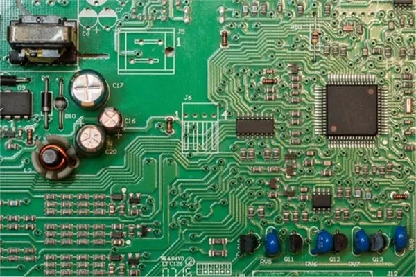


抖音二維碼

Q Q二維碼

微信二維碼
點擊
然后
聯系
然后
聯系
電話熱線
13410863085Q Q

微信

- 郵箱