鑫景福致力于滿足“快速服務,零缺陷,輔助研發”PCBA訂購單需求。


PCB制造
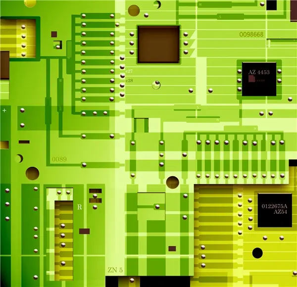
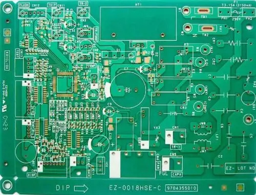
The circuit board makes the circuit miniaturized and intuitive, and plays an important role in the mass production of fixed circuits and the optimization of the layout of electrICal appliances.
Homemade process
One, print circuit board
The printed circuit board will be drawn with transfer paper, pay attention to the slippery side facing yourself, generally print two circuit boards, that is, print two circuit boards on a piece of paper. Choose the best printed circuit board.

Cut copper clad sheet
The whole process diagram of making a circuit board with a photographic plate. Copper coated board, that is, both sides of the circuit board covered with copper film, copper coated board cut into the size of the circuit board, not too large, in order to save material.
Pretreated copper clad sheet
Use fine sandpaper to polish off the oxide layer on the surface of the copper coated plate, to ensure that when the circuit board is transferred, the toner on the thermal transfer paper can be firmly printed on the copper coated plate, and the standard of polishing is that the surface is bright and there is no obvious stain.
Transfer printed circuit board
Cut the printed circuit board into a suitable size, paste the printed side of the circuit board on the copper coated plate, align the copper coated plate into the heat transfer machine, put it into the transfer paper must ensure that there is no dislocation. Generally speaking, after 2-3 transfer, the circuit board can be firmly transferred to the copper coated plate. The heat transfer machine has been preheated in advance, the temperature is set at 160-200 degrees Celsius, because the temperature is very high, pay attention to safety when operating!
First check whether the circuit board is complete transfer, if there are a few not good transfer can be repaired with a black oil pen. Then it can be corroded, such as the circuit board exposed copper film is completely corroded away, the circuit board from the corrosion liquid to remove clean, so a circuit board corrosion good. Corrosion liquid ingredients for strong hydrochloric acid and hydrogen peroxide, and water, ratio of syntactic sugar for 1:2:3, when mixed corrosion liquid, water first, again add concentrated hydrochloric acid, hydrogen peroxide, if the operation is concentrated hydrochloric acid, hydrogen peroxide or corrosion solution accidentally splashed on the skin or the clothes to wash immediately with water, because you want to use the corrosive solution, operation must pay attention to safety!
The circuit board is to insert electronIC components, so you have to drill holes in the circuit board. Choose different drill pins according to the thickness of electronic component pins. When using the drill to drill, the circuit board must be stable. The speed of the drill can not be too slow.
After drilling, sand the toner covered on the circuit board with fine sandpaper and clean the circuit board with water. After the water is dried, the rosin water is applied to the side with the circuit. In order to speed up the solidification of the rosin, we use a hot fan to heat the circuit board. It only takes 2-3 minutes for the rosin to solidify.
Industrial process
production process of double-sided tin plate/sunk gold plate:
Cutting -- -- -- -- -- -- -- -- -- -- -- drilling sink copper etching figure - - the line - - resistance welding - character - tin (or a heavy gold) - gong side - cut v (some plate don't need to) -- -- -- -- -- -- fly test vacuum packing
Double-sided gold plate production process:
Cutting -- -- -- -- -- -- -- -- -- -- -- drilling sink copper - line - gold-plated figure - electricity - etching - resistance welding - character gong side -- -- -- -- -- -- -- -- - v - cut flying test vacuum packing
Production process of multi-layer tin plate/sunk gold plate:
Open -- -- -- -- -- - the inner material -- -- -- -- -- laminated - drilling - heavy copper etching figure - - the line - - resistance welding - character - tin (or a heavy gold) - gong side - cut v (some plate don't need to) -- -- -- -- -- -- fly test vacuum packing
Multi-layer gold plate production process:
Open -- -- -- -- -- - the inner material -- -- -- -- -- laminated - drilling - sink copper - line - figure - plating, etching, resistance welding - character gong side -- -- -- -- -- -- -- -- - v - cut flying test vacuum packing
Profile control system processes
1. Remove the devices on the original board.
2. Scan the original board to get the graphic file.
3. Grind off the surface layer to get the middle layer.
4. Scan the middle layer to get the graphic file.
5. Repeat steps 2-4 until all layers have been processed.
6. Use special software to convert graphic files into electrical relation files --PCB diagram. With the right software, the designer can SIMply trace the figure over.
7. Check and complete the design.
layout
The layout design should be noted as follows:
Single panel
This type of panel is usually used when the cost requirements are low. In layout design, it is sometiMES necessary to use components or jumper cables to skip circuit board wiring. If there are too many, you should consider using dual panels.

Double panel
Dual panels can be used with or without PTH. Because PTH boards are expensive, they are used only when the complexity and density of the circuit require it. In layout design, the number of wires on the component surface must be kept to a minimum to ensure easy access to the required materials.
In PTH boards, plated through-holes are used only for electrical connections and not for installation of components. For reasons of economy and reliability, the number of holes should be kept to a minimum.
When choosing a single panel or a double panel, it is important to consider that the surface area of the component (C), which is in an appropriate constant ratio to the total area of the printed circuit board (S), is useful for component installation. It is worth noting that "US" usually refers to the area of one side of the panel. Table 3-2 lists the S: C ratio ranges for the most commonly used printed circuit boards.
6
To make content
Introduction to the
When the circuit board is made, the relationship between the diameter of the pad and the maximum width of the wire is needed, so as to make a good circuit board, circuit board,PCB board factory, aluminum substrate, high-frequency board,PCB and so on.
Relationship between
Diameter of pad (in. /Mil/ mm) Maximum wire width (in. /Mil/ mm)
0.040/40/1.015 0.015/15/0.38
0.050/50/1.27 0.020/20/0.5
0.062/62/1.57 0.025/25/0.63
0.075/75/1.9 0.025/25/0.63
0.086/86/2.18 0.040/40/1.01
0.100/100/2.54 0.040/40/1.01
0.125/125/3.17 0.050/50/1.27
0.150/150/3.81 0.075/75/1.9
0.175/175/4.44 0.100/100/2.54
Small fast circuit board plate making system
10-31,2022


抖音二維碼

Q Q二維碼

微信二維碼
點擊
然后
聯系
然后
聯系
電話熱線
13410863085Q Q

微信

- 郵箱