鑫景福致力于滿足“快速服務(wù),零缺陷,輔助研發(fā)”PCBA訂購單需求。


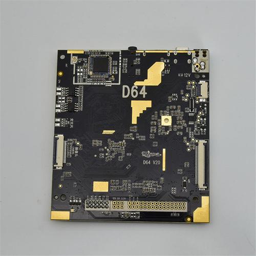
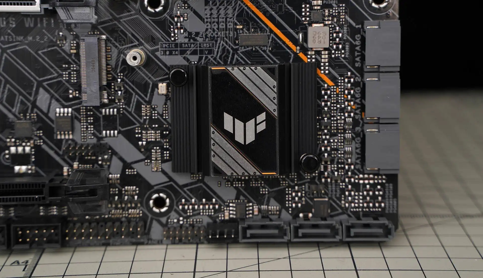
PCB制造
It is not easy to make circuit boards. Some gadget enthusiasts like to design and create their own printed electrIC boards, but they don't like the finished aspects of the machine. Besides, it takes a lot of time to make a lot of boards at home. Let us know during the Circuit board assembly process to give you a better idea of how the device is created in detail.
As long as you fuse the electronic device to the printed circuit board, assemble and fabricate it. However, the panel assembly differs from its manufacture. Along with PCB production, there are several steps involved, including designing the PCB and prototyping the PCB.

It is very important to collect all the correct equipment and install it on the board before plugging in the electronics. The question now arises as to what PCB is instalLED in which device. Different electronic boards have different components involved, depending on what is to be installed on the device. There are two main types of manufacturing methods involved in making PCB assemblies:
1) Hole through method: In this method, the device is implanted into the hole
2) surface mount method: In this method, the external plane of the electronic circuit board mounted on the device.
The device is mounted on a printed circuit board with the help of metal solder through the use of electricity. The capacity of the board determines how the device must be fused on the board. In the case of manufacturing a larger number of board components, it is always best to use the machine. The circuit is placed on the machine by wave soldering as well as by using a reflow furnace. Bulk wave soldering or reflow soldering furnace is placed on the machine. In the case of SMAll-scale production, hand welding is always an option.
SometiMES the two hole through method as well as the surface mount method are applied in a single assembly, because some electronIC components are only available in the hole through the sleeve, while others are only available in the surface mount package. The method was used in the assembly process when it proved to be advantageous.
Mounting holes through powerful electronic components, in case they have certain physical damage. However, it is better to make use of the surface mount method when you know that any damage is unlikely to occur. The surface mount method uses an electronic board with less area.
As long as the assembly process, it is important to check that the motherboard is working properly and performing the required functions. In the case of a fault on a part of the printed circuit board, it is easy to identify the problem and the source of replacement can be done.
Chilag Patel is a creative content writer who works on Muncie research. He blogs PCB design, consumer electronics, Automotive electronics and many more.
Inspection of assembled printed circuit boards
To meet the requirements of PCB testing, a variety of testing equipment has been produced. Automatic optical inspection (AOI) system is usually used to test the inner layer before the formation of layers. After layering, the X-ray system monitors alignment accuracy and minor defects; The scanning laser system provides a method for detecting the pad layer prior to reflux. These systems, together with visual inspection technology on the production line and component integrity testing with automatically placed components, help ensure the reliability of the final assembly and welded plates.
However, even if these efforts minimize defects, there is still a need for final inspection of the assembled PCB, which is perhaps the most important because it is the final unit of product and process evaluation.
Final inspection of assembled printed circuit boards may be done either by dynamic methods or by automated systems, and both methods are often used. "Manual" means that an operator uses an optical instrument to visually inspect the board and make a correct determination about the defect. Automated systems use computer-aided graphic analysis to determine defects, and many people also believe that automated systems contain all detection methods except manual light detection.

X-ray techniques provide a method for estimating solder thickness, distribution, internal voids, cracks, dessoldering and the presence of solder spheres (MARKstein, 1993). Sonography will detect holes, cracks, and unglued joints. Automatic optical detection * Estimation of external features, such as bridging, tin melt and shape. Laser detection can provide three-dimensional images of external features. Infrared detection detects internal weld faults by comparing the thermal signal of the weld with that of a known good weld.
It is worth noting that these automatic detection techniques have been found for all defects that the limited detection of assembled printed circuit boards cannot detect. Therefore, the manual visual detection method must be used in conjunction with the automatic detection method, especially for those few applications. The combination of X-ray detection and manual optical detection is the best method to detect defects of assembly plates.


抖音二維碼

Q Q二維碼

微信二維碼
點擊
然后
聯(lián)系
然后
聯(lián)系
電話熱線
13410863085Q Q

微信

- 郵箱