鑫景福致力于滿足“快速服務,零缺陷,輔助研發”PCBA訂購單需求。


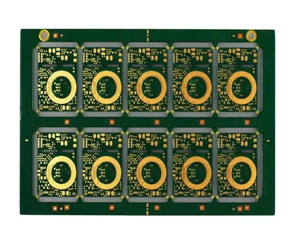
PCB制造
Requirements of press fit assembly circuit board and acceptance of protective coating
The basIC idea of using push in adapter connector is to closely match with the through-hole size of the circuit board. Therefore, the stability of the characteristic size of the circuit board is the key to the successful use of the whole connection system.
The final metal surface treatment of the plated through-hole on the circuit board will have a significant impact on the contact force between the pressed pin connector and the hole wall. The hole wall coated with soldering tin provides lubrication, which can help the tip enter the plated through hole smoothly. When the final metal surface is treated with tin lead or pure tin, the circuit board manufacturer should be careful that too much metal remains in the hole to affect the hole diameter. Too thick surface treatment will cause the connector installation to be planed off, and the crack may relax and cause electrical short circuit.
Fusible coating, such as tin or tin lead, may also produce a convex surface in the electroplated through-hole in the subsequent SMT or wave soldering thermal cycle. This convex face may change the hole diameter, resulting in excessive pressure demand, or may increase the tendency of solder flakes. Holes with high aspect ratio (circuit board thickness/through-hole diameter) may have too high electrical release thickness at the hole edge of the surface layer of the circuit board, but have too thin precipitation thickness in the middle of the plated through-hole, which is caused by insufficient through-hole capacity of the plating bath. Typical results of three through-hole electroplating are shown in the attached figure.
The influence of the through hole metal thickness on the subsequent press fit assembly is as follows:
? If the hole wall is too thick, the pressing force may exceed the mechanical strength of the cuttings, and the cuttings may be at risk of bending.
? If the applied force is too large than the bearing force of the circuit board structure, it may damage the circuit board, cause the hole wall to break, affect the connection, damage the interconnected circuit, or even wear out the hole ring.
? The force of pressing the terminal through the smooth area of the connector may be enough to break through the too thin hole wall metal.
The final metal treatment shall be carefully selected, which is relatively important for controlling the hole wall thickness of the circuit board. The thickness of copper flux treatment can be well controlLED except for holes with high aspect ratio, which is SIMilar to other final metal surface treatment. However, due to the lack of lubrication essence, bare copper is relatively difficult to make the insert smoothly pressed compared with the final metal surface treatment of nickel/gold, tin lead and silver.
On the whole, controlling the diameter stability of the through-hole, the durability of metal treatment, and the compatibility with the pin pressing are the most important things for circuit board manufacturing.
How to check and accept the protective coating of Circuit board assembly?
During the manufacturing process of circuit board manufacturers, not all pcb assembly designs will use protective coating, but when used, they must meet the subsequent acceptance specifications. If wave soldering or tin bath is used to install and solder the parts to the printed circuit board, all these printed circuit board assemblies will be made by covering the solder stop paint with the top or bottom etched lines. Without solder stop paint, soldering tin will cause bridging between conductors, leading to uncontrollable problems.
Protective coating is a kind of insulation protective coating, which protects the structures coated after the PCB is assembled. Protective coating shall be uniform, transparent and colorless. The protective coating shall be polymerized correctly without showing viscosity.
Protective requirements for three types of protective coating thickness are listed below:
(1) Type ER (epoxy resin), UR (carbamate), AR (acrylic) 0.05? 0.08mm
(2) Type SR (silicone) 0.08? 0.13mm
(3) Type XY (p-xylene) 0.01? 0.05mm
The thickness can be measured with samples made at the same time as the assembly, and the pin ends do not need protective coating. Solder stop paint is a kind of film coating, which is used as dielectric and mechanical shielding during and after welding operation. Solder stop paint materials can be made of liquid or dry film.
For the first and second level of product equipment, the operation fracture of thick welding and cleaning stop paint is acceptable, but it is unacceptable in the third level. After assembly, welding and cleaning operations, as long as the solder stop paint does not float, crack, peel or fall off on the printed circuit board, it is acceptable for the solder stop paint to generate wrinkles on the tin lead plated lines. Cracking, peeling or dropping of solder stop paint on PCB assembly is unacceptable, and crimped solder stop paint after assembly is unacceptable on bare copper circuit.


抖音二維碼

Q Q二維碼

微信二維碼
點擊
然后
聯系
然后
聯系
電話熱線
13410863085Q Q

微信

- 郵箱