鑫景福致力于滿足“快速服務,零缺陷,輔助研發”PCBA訂購單需求。


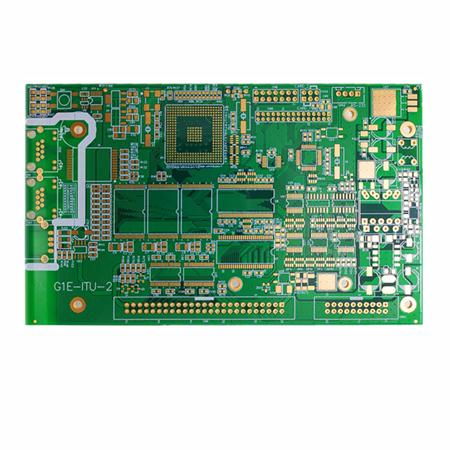
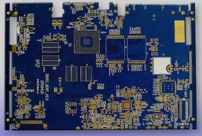
PCB制造
With the increase of speed, EMI becoMES more and more serious, and it is manifested in many aspects (such as electromagnetIC interference at the interconnection). High speed devices are particularly sensitive to this, so they will receive high-speed false signals, while low-speed devices will ignore such false signals.
At the same time, EMI also threatens the security, reliability and stability of electronic equipment. Therefore, when designing electronic products, PCB design is very important to solve EMI problems.

Electromagnetic interference (EMI)
Electromagnetic interference (EMI) can be divided into radiation and conduction interference. Radiated interference means that the interference source interferes its signal to another electrical network with space as the medium. Conducted interference refers to the interference of signals on one electrical network to another electrical network by using conductive medium as the medium. In high-speed system design, integrated circuit pins, high-frequency signal lines and various plugs are common radiated interference sources in PCB design. The electromagnetic wave they emit is electromagnetic interference (EMI), which will affect the normal operation of themselves and other systems.
PCB design Skills for EMI
1. Common mode EMI interference source (such as the voltage drop formed by the transient voltage formed on the power bus at the two ends of the inductance in the decoupling path)
When low value inductors are used in the power supply layer, the transient signal synthesized by the inductors will be reduced, and the common mode EMI will be reduced.
Reduce the length of the wiring from the power layer to the IC power supply pin.
Use 3-6 mil PCB layer spacing and FR4 dielectric material.
2. Reduce loop
Each loop is equivalent to an antenna, so we need to minimize the number of loops, loop area and loop antenna effect. Ensure that the signal has only one loop path at any two points, avoid artificial loops, and try to use the power layer.
3. Filtering
Filtering can be used on both power lines and signal lines to reduce EMI. There are three methods: decoupling capacitor, EMI filter and magnetic element. The EMI filter is shown in the figure below.
4. Electromagnetic shielding
The signal wiring shall be placed on the same PCB layer as far as possible and close to the power supply layer or ground plane.
The power layer shall be as close to the ground plane as possible
5. Layout of parts (different layouts will affect the interference and anti-interference capability of the circuit)
Block processing shall be carried out according to different functions in the circuit (such as demodulation circuit, high-frequency amplification circuit and frequency mixing circuit). In this process, strong and weak electrical signals shall be separated, and digital and analog signal circuits shall be separated.
The filter network of each part of the circuit must be connected nearby, which can not only reduce the radiation, but also improve the anti-interference ability of the circuit and reduce the chance of being interfered.
The easily disturbed parts shall be arranged to avoid interference sources as much as possible, such as the interference of CPU on the data processing board.
6. Consideration of wiring (unreasonable wiring will cause cross interference between signal lines)
There shall be no wiring close to the frame of PCB board to avoid wire breakage during fabrication.
If the power cord is wide, the loop resistance will be reduced.
The signal line shall be as short as possible and the number of vias shall be reduced.
The right angle method cannot be used for wiring at corners, and 135 ° angle is preferred.
The digital circuit and analog circuit shall be isolated by ground wire, and the digital ground wire and analog ground wire shall be separated, and finally connected to the power supply ground.
7. Increase the dielectric constant of PCB/increase the thickness of PCB
Increase the dielectric constant of the PCB board to prevent the transmission line near the board and other high-frequency parts from radiating outward; Increasing the thickness of PCB board and minimizing the thickness of microstrip line can prevent the overflow of electromagnetic lines and also prevent radiation.
PCB Design Method and Key Points Analysis
11-06,2022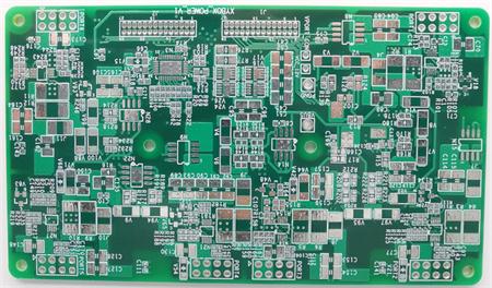


抖音二維碼

Q Q二維碼

微信二維碼
點擊
然后
聯系
然后
聯系
電話熱線
13410863085Q Q

微信

- 郵箱