鑫景福致力于滿足“快速服務(wù),零缺陷,輔助研發(fā)”PCBA訂購單需求。


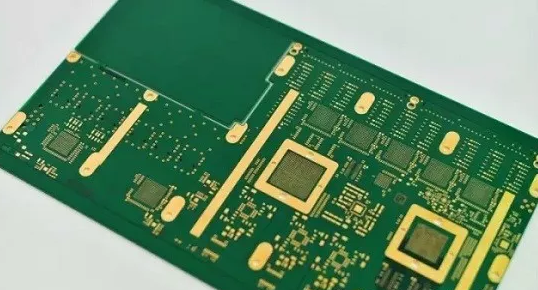
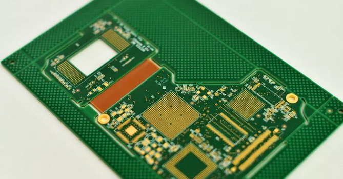
PCB制造
Hole breakage and copper partICles on hole wall during PCB production
In case of hole breakage, copper particles and copper wires on the hole wall in the copper manufacturing process, which slots have problems? What is SAP process?
The primary copper, as defined by the general industry, refers to the three processes as a whole, namely, glue removal slag, chEMIcal copper and full plate electroplating. Hole breaking, copper particles and copper wires in the hole wall are often not a copper problem, but a problem caused by chemical copper precipitation or glue removal slag process. In the process of removing the glue residue, the circuit board will go through three liquid medicine treatment procedures: bulking agent, oxidant and reductant. If the liquid medicine is aged in the reduction process, permanganate residues may not be completely removed on the hole wall. When this kind of circuit board enters the chemical copper process, it will be attacked by the micro etching solution and will fall off locally. At this time, the active layer established by the pore forming agent will be damaged, resulting in the poor growth of the chemical copper and hole breakage.
Of course, the chemical copper process itself may also cause hole breaking problems, such as insufficient chemical copper activity, too high hole depth, and problems with the use of hole cleaners and palladium colloids, which will also affect the quality of the hole wall. If the drilling quality is poor, hole breakage is more likely to occur, especially if the hole wall is too thick, which will lead to poor cleaning, residual liquid affecting chemical copper precipitation and other problems, especially easy to cause hole breakage.
As for electroplating problems such as copper particles and copper wires, the common problem sources are poor brushing and grinding, chemical copper roughness and other factors. In terms of improving chemical copper, it is feasible to improve the integrity of water washing, stripping rack and liquid medicine replacement. In particular, it is necessary to avoid mixing chemical copper micro etching with stripping rack treatment tank. Such problems often occur in factories with limited foundry and work site. When the two are used together, the colloid left after stripping rack treatment will be separated in the hole, resulting in rough hole wall. From this point of view, to eliminate such roughness, we should not only avoid tank mixing, but also pay attention to palladium colloid and water washing filtration circulation system, so as to minimize the chance of hole wall roughness.
The manufacturer can also consider using the direct electroplating process when the product allows. There is no palladium colloid problem in this type of process. However, some system providers limit the use of this type of technology because of the circuit board structure and past historical experience. This is the first part to consider when setting up the process. Shadow, BlackHole and other processes are representative of this kind of technology, and may also have the function of improving the problem of copper particles on the hole wall.
The full name of SAP is "SemiAdditive Process", because there are two methods for general circuit fabrication: full etching and partial etching and partial circuit electroplating. This method of partial etching has strong circuit making ability and can be used to make thinner circuits. Therefore, if the external circuit of the general circuit board has a detaiLED circuit design, it may be considered to use the SAP process to make the circuit. In recent years, the requirements for circuit fabrication have become more and more precise, so some circuit boards are fabricated based on all chemical copper. At present, most of the industry say that the so-called SAP process refers to such practices.
In fact, all methods of circuit electroplating can be called SAP process, but their base copper thickness is different. However, at present, the industry believes that only the process of base copper being pure chemical copper should be called SAP process. In addition, in the field of structural loading plates, some manufacturers also use ultra-thin copper sheets to make circuits. At this time, a different name "M-SAP" is added. This M refers to metal, which means copper metal. At this time, the manufacturing process is no longer pure chemical copper base, but ultra-thin copper sheets. PCB manufacturers, PCB designers and PCBA processors explain that PCB production has holes and copper particles on the hole wall.


抖音二維碼

Q Q二維碼

微信二維碼
點擊
然后
聯(lián)系
然后
聯(lián)系
電話熱線
13410863085Q Q

微信

- 郵箱