鑫景福致力于滿足“快速服務,零缺陷,輔助研發”PCBA訂購單需求。


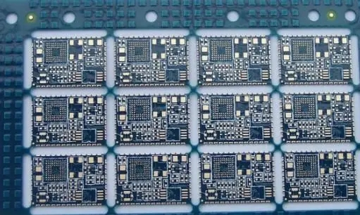
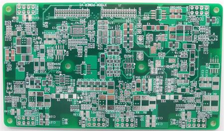
PCB制造
Discussion on the Half Plug Hole Method of PCB Printed Circuit Board
1. Preface
In production, some customers sometiMES require that some holes be plugged, but they cannot be fully plugged. The back of the plug hole is solder blocked and has depth requirements, whICh is commonly known as "PCB half plug hole". It is understood that such customers want to test in these holes and will drive the test probe into the holes. If there is too much ink in the hole, or the hole wall is polluted by ink, it is easy to cause a false open circuit and affect the test results; If the amount of ink in the hole is too SMAll, or the hole is not plugged, it cannot meet the requirements of the hole.
Therefore, the depth of the plug hole must be controlLED in the pcb production process, and the plug hole shall be made according to the depth required by the customer. From the experience of conventional green oil plug hole, it is known that the difficulty of controlling the depth of plug hole is not that the plug is not enough, but that a relatively small plug hole depth and the accuracy of the specified plug hole depth. At present, there are two main methods. One is to fill the hole plug or a certain depth, then the back of the hole plug is not exposed, and part of the ink is washed away through development to achieve a certain depth of the hole plug; The second is to strictly control the depth when plugging holes, and then both sides of the holes are exposed. The two methods are tested below.
2. Experimental methods
The thickness of the test plate is 2.4 mm, and the aperture is 0.25, 0.30, 0.40, 0.50 mm. Use flat screen printing machine to plug holes. After the test, the metallographic section shall be made for the plug hole, the effect of the plug hole shall be observed through the metallographic microscope, and the copper exposure depth shall be measured.
3. Results and discussion
3.1 Development parameters control the plug hole depth
Test process: pre-treatment → CS side plug hole (full) → pre drying → silk screen double-sided → pre drying → exposure (level 11, SS windowing CS cover oil) → development → curing → detection
When all the holes are filled, the ink for the solder mask hole plug will be washed away by the developer after the developer. The development control parameters mainly control the depth of the plug hole through the development time. The experimental results are shown in Figure 1. Under the normal development time of 80 seconds, 0.25 and 0.3 mm holes can flush out the ink with a depth of 0.5~0.6 mm, that is, the depth of exposed copper, while 0.4 and 0.5 mm holes can flush out the ink with a depth of 0.6~0.8 mm. Therefore, the development can wash off part of the ink in the plug hole. Prolonging the development time and increasing the development times can flush out more ink in the hole, but the ink in the hole with the same development time or development times and small aperture is difficult to flush out. Because the developing solution with small aperture is not easy to interact with the ink, the ink depth in the hole is large and the exposed copper part is small.
However, this method has the following problems: because the ink in the hole is not completely dried, there are a lot of solvents, and these solvents are not dissolved by the developer, it is easy to cause ink pollution on the board, and these inks are not easy to clean and find, which brings great inconvenience to production. In actual production, the development time is controlled between 80-120s. During this time, different apertures can flush out different inks. The ink that can be flushed out by small apertures is limited. If the customer requires a plug hole depth of 50% (taking 2.4mm plate thickness as an example), it is difficult to achieve this. Moreover, the accuracy and uniformity are difficult to control.
3.2 Plug hole parameter control depth
Test process: grinding plate → CS plug hole → pre drying → SS exposure (level 17, aluminum sheet of plug hole is used as film) → silk screen on both sides → pre drying → exposure (level 11, SS windowing CS cover oil) → development → thermal curing.
The plane plug hole machine can control the depth through a lot of plug hole parameters, including the number of plug hole cutters, tool feed speed, plug hole pressure, etc. The main rules are as follows: the less the number of hole stoppers is, the less the hole stoppers are; The faster the cutting speed of the plug hole, the less ink in the hole; The higher the scraper height, that is, the lower the pressure, the less ink in the hole; In addition, under the same parameters, there is less ink in the small aperture hole. In this test, it is often necessary to adjust multiple parameters to make the plug hole depth meet the required requirements. Table 1 lists the plug hole effects at different cutting speeds when the plug hole pressure is small.
Table 1 Copper Exposed Depth at Different Tool Speed (Unit: mm)
Tool feed speed m/min 0.25mm 0.3mm 0.4mm
10 1.34 1.16 0.89
30 1.51 1.34 1.18
50 1.65 1.49 1.32
The test result is that since the hole is exposed before development, the plate surface is clean during development, and the depth of the plug hole can be well controlled. It can be seen from the above table that the exposed copper depth can reach 1.65mm for 0.25mm aperture; The 0.3mm hole is about 1.49mm; 0.4mm hole is within 1.32mm. Fig. 4 is the metallographic photo of 0.3mm PCB half plug hole controlled by plug hole parameters. If you want to make the ink in the hole less, you can make the cutting speed faster. In addition, you can adjust the air supply pressure, aluminum sheet aperture size, scraper angle, etc.
4. Conclusion
The first method achieves the depth control of the plug hole by developing and flushing out part of the ink in the hole, which has the advantages of SIMple process and operation, while the disadvantage is that the ink often pollutes the board surface when developing; The depth is affected by the development parameters. It is difficult to reach the optimal value at the same time because it is necessary to consider both the control depth and other conditions of plate development in production; In addition, the uniformity is relatively poor. The second method has a long process and is relatively complex to make. Before mass production, it is often necessary to make a first plate to confirm whether the depth is appropriate, but there is no need to worry about the plate surface being polluted after development. Two methods are used to make the ink shape diagram in the plug hole. It can be seen that there are more copper exposed parts under the same depth of the direct plug hole control, which is conducive to the customer's test. In the production, the author believes that two production methods should be properly selected and adjusted according to the production output to save costs and improve production efficiency.
PCB manufacturing, PCB design, PCBA processing manufacturers will explain to you the discussion of PCB half plug hole method.


抖音二維碼

Q Q二維碼

微信二維碼
點擊
然后
聯系
然后
聯系
電話熱線
13410863085Q Q

微信

- 郵箱