鑫景福致力于滿足“快速服務,零缺陷,輔助研發(fā)”PCBA訂購單需求。


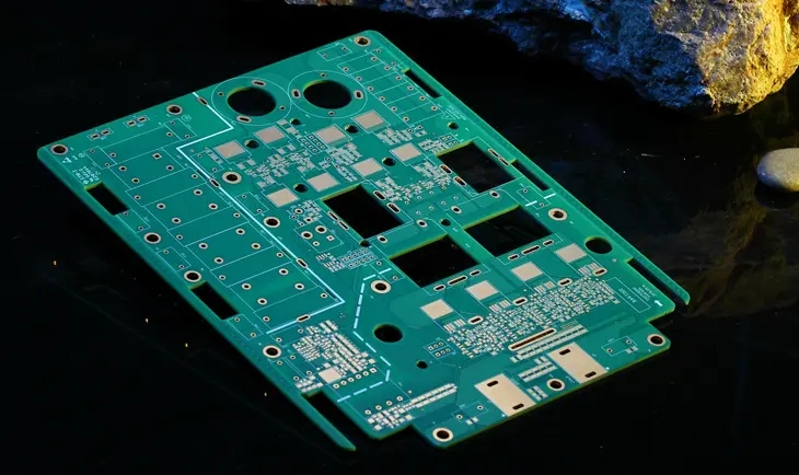
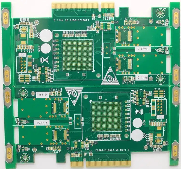
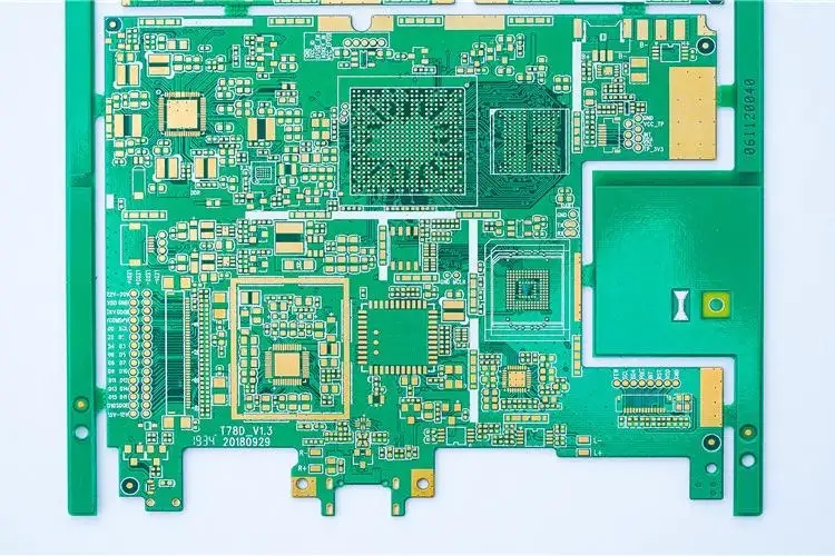
PCB制造
DetaiLED explanation of flexible circuit board manufacturing for PCB proofing
PCB manufacturing, PCB design, PCBA processing manufacturer will explain the manufacturing of flexible PCB for PCB
Pcb proofing let's talk about manufacturing documents, whICh are very important. We tell manufacturers what we want through manufacturing documents. However, they are also important factors that cause misunderstanding or mistakes, leading to costly delays. Fortunately, we can refer to some standards to ensure that our communication with the manufacturer is unimpeded.
This can be summarized as the following golden rules:
Make sure your manufacturer has the ability to manufacture the hard and soft combination boards of your design.
Make sure they work with you from the time they build the casCADing structure, so that the design can meet their production process.
Let them participate in the design process as early as possible.
Pcb proofing output data set
After visiting some local board makers who are capable of making soft and hard composite boards, we found that many designers still send gerber files to their board makers. However, ODB++v7.0 or higher should be preferred because GenFlex? And SIMilar CAM tools can clearly identify the specific layer type. As shown in Table 1, the included data subset.
Discussion on Manufacturing Documents of Flexible circuit board
If we use Gerber or earlier versions of ODB++, we will encounter a lot of trouble. In other words, the manufacturer needs to separate the cutting path and die cutting pattern of the rigid and flexible circuit parts. In fact, we need to use mechanical film to show the avoidance requirements on the hard board and which parts of the flexible circuit area will be exposed; Shows how to use overlays to strengthen pads for components mounted on flexible circuits.
In addition, special attention should be paid to the drilling pairs and through-hole plating pairs, because the drilling from the rigid plate to the reverse side of the flexible plate requires re drilling, which will increase costs and reduce production.
As a designer, the real question is, how do you define these areas, layers, and stacks?
Pcb proofing uses tables to define stacked stacks
The most important documents provided to manufacturers are undoubtedly stacked. In order to make a soft and hard combination board, it is also necessary to provide different stacks in different fields and clearly identify them. A simple method is to copy the outline of the board on the mechanical layer, MARK the areas with different stacks, and put the corresponding stack structure table aside.
In this example, I used different stack area matching patterns to indicate which layers are included in the flexible part or the rigid part. It can be seen that the "insulation layer 1" here uses FR-4 because it is a reinforcing plate.
This has created new problems. We also need a 2D space to define where is bent or folded, where components and other important objects can pass through the boundary between rigid and flexible. I will elaborate on this later.
PCB design intent of pcb proofing transfer
As we all know, pictures are worth a thousand words. If we can generate a 3D image showing flexible and rigid areas, it will help manufacturers understand our intentions more clearly. Now many people use MCAD software to realize this view, and they import the STEP file of PCB design into MCAD software.
The other advantage is that it can help us check the mutual interference between flexible plates and between flexible plates and rigid plates to avoid huge mistakes.
Placement of pcb proofing components
As can be seen from the above figure, the soft and hard combination board means that components can be placed in the middle layer, not just the top layer and bottom layer. This is a bit tricky in PCB design software, because usually components must be placed at the top and bottom. Therefore, we need the ability to place components in the middle layer.
Fortunately, AlTIum Designer can place pads on any layer, so this is possible. In addition, silk screen can be printed on flexible circuits. This is not a problem, because the coating material can be well bonded with screen printing ink. The key is to select enough ink color with strong contrast through the coating material. The clarity of silk screen will be affected because it needs to pass through the covering film and the SMAll spacing between them. Again, we need to consult with manufacturers to find a feasible and economic approach.
Note: If we plan some areas on the PCB to connect flexible boards and place components on these areas, then this is a reasonable area to place embedded components. We need to generate a set of very clear documents to show the location of the incision and the layered structure. This will be limited by the manufacturing method, such as re drilling or multiple pressing. Therefore, it is very important to accurately communicate your intentions and minimize the number of separate openings. It is better to avoid crossing openings on both sides of the board.
PCB manufacturing, PCB design and PCBA processing manufacturers will explain the manufacturing of flexible PCB for pcb proofing.


抖音二維碼

Q Q二維碼

微信二維碼
點擊
然后
聯(lián)系
然后
聯(lián)系
電話熱線
13410863085Q Q

微信

- 郵箱