鑫景福致力于滿足“快速服務,零缺陷,輔助研發”PCBA訂購單需求。


PCB制造
With the current increase in PCBA capabilities and SMAller sizes, you can assume that single-layer boards are effectively obsolete. In fact, these boards are used in many common products such as printers, digital CAMeras, calculators, stereos, and some power supplies. Nonetheless, multi-layer PCB stack-ups are on the rise and are generally preferred over single-layer PCBAs.
As the number of uses for electronic circuit boards has grown—in line with the need for greater functionality and higher capabilities—the variety of installation environments has also increased. Make the most of your PCB layers when designing boards with size constraints; including layer count, stackup arrangement, number and type of vias, and other design specifICations. To do this, you need a solid understanding of the multilayer PCB manufacturing process.

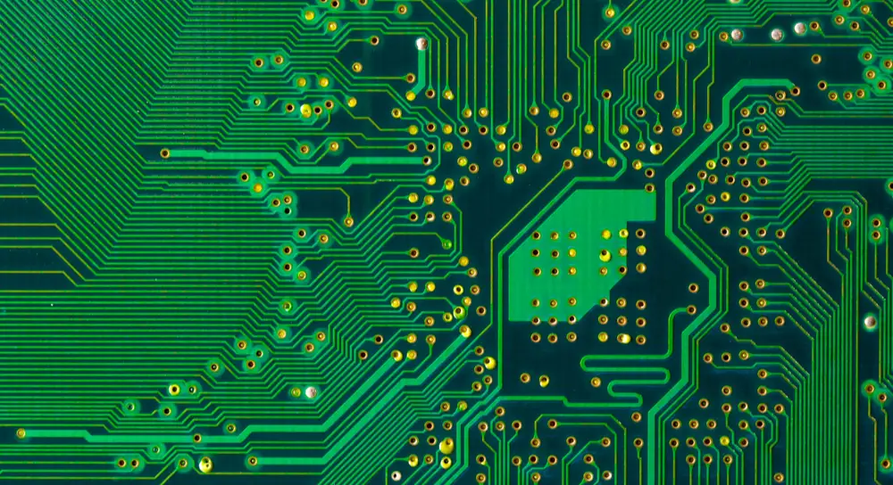
Multilayer PCB Manufacturing Process
The basic steps for building and assembling a PCB, whether single-layer, double-layer, or multi-layer, are SIMilar and listed below.
PCBA manufacturing process steps
Create images, remove unwanted copper (etch) from inner layers, align and insulate layers and stacks, drill holes for vias and mounts, etch outer (top and bottom) layers, in plated through hole (PTH) walls Add copper on top, add solder mask to protect the board, print silkscreen MARKs, add surface treatments to protect copper surface areas (e.g. traces, keep out, guard rings)
Assembly steps
Apply solder paste to prepare for soldering, pick and place SMT components, send board through reflow oven, view solder joint quality and rework if necessary, mount through-hole components, solder through-hole components to board, if necessary, Perform inspection and final THT soldering, clean boards to remove debris and other contaminants, panels or separate into individual PCBAs, perform final quality checks.
The multi-layer PCB manufacturing process includes all of the above steps; however, other considerations also arise that do not exist for single- and double-sided boards.
Multilayer Specific PCB manufacturing Issues
As mentioned earlier, adhering to size constraints is the main reason and advantage of using a multilayer PCB design. Reducing signal length is another advantage, which is critical for reducing EMI. For example, multiple layers provide additional circuit paths, allowing for more complex designs. Additionally, smaller form factors are generally more durable and reliable, minimizing the chance of premature failure after deployment.

These properties are built into the multilayer PCB manufacturing process through the use of various types and sizes of materials through options, including blind via, buried via, and through-pad via options. multilayer boards are also rigid and have better inherent structural integrity than flexible or rigid-flex PCBs. It must be noted, however, that for high-level boards, several successive lamination cycles may be necessary. In these cases, your choice of board material and other design decisions become even more critical, as many materials are limited to four or fewer cycles before delamination or board damage can occur.
Designed to optimize Multilayer board builds
Building the best multilayer PCBA is a joint exercise and is best accomplished through white box fabrication. This will ensure that your design is manufacturable and will accurately reflect your design intent. Following the guidelines listed below will Help your multilayer PCB manufacturing process achieve these goals.
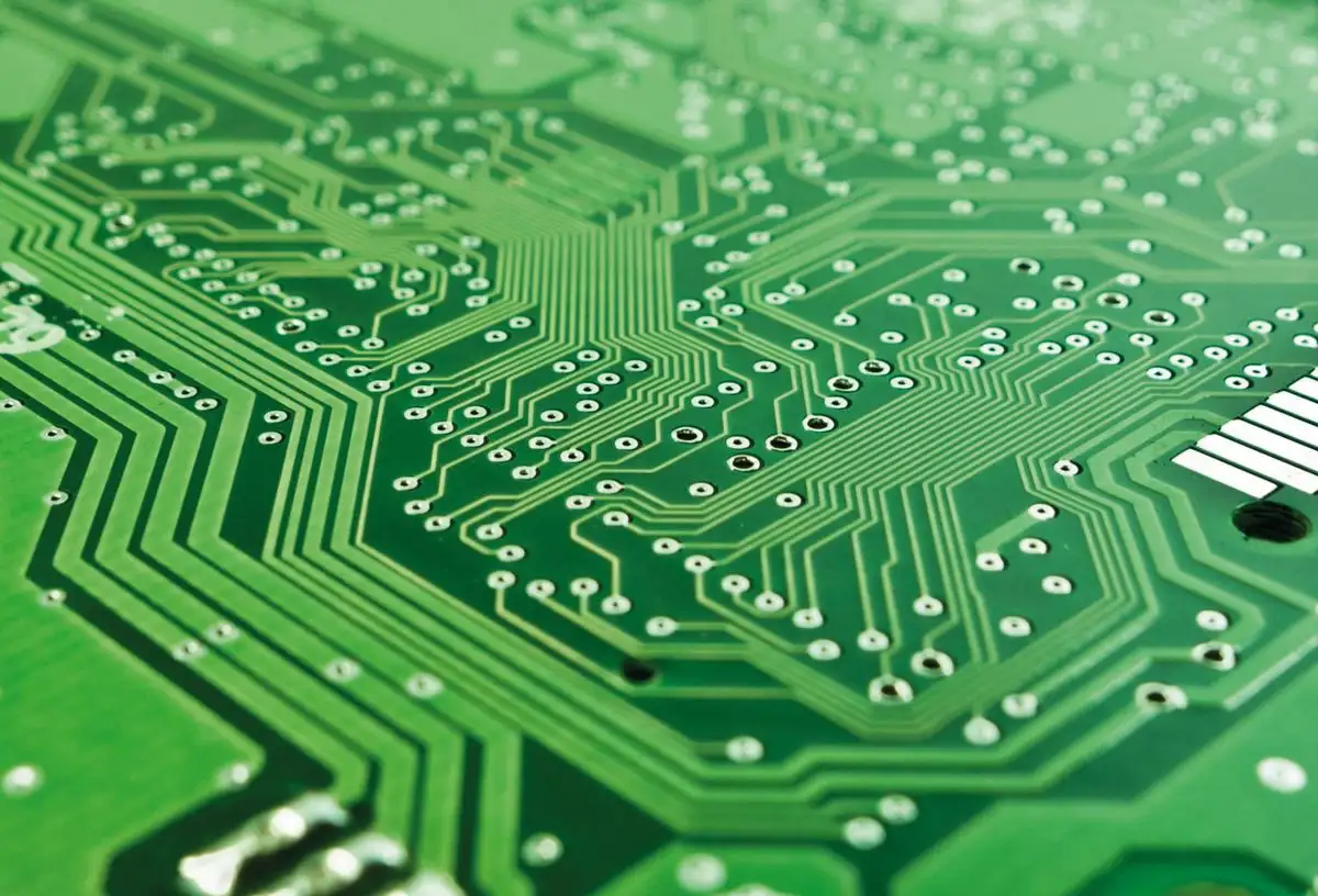
Design Guidelines for Multilayer PCB Manufacturing Process Optimization
Materials are selected based on application and manufacturing requirements, and while FR-4 is a good general-purpose material, selecting materials based on how the board is constructed and used is a better design choice. Use the largest acceptable size board The largest board area should give you the best chance of meeting clearance and spacing requirements. Use the simplest possible vias and follow sizing rules and guidelines.
Although vias run vertically through your board structure, as opposed to surface traces routed horizontally, size and spacing are important considerations. Misusing vias can overcomplicate your design and put a lot of unnecessary stress on your multilayer board build process.
The optimal PCB stack-up is symmetrical and contains a sufficient number of layers to separate signal types and ground planes. The list above provides a solid foundation for your multilayer board build. At Rhythm Automation, as the industry leader in rapid, high-quality prototyping and on-demand PCBA manufacturing, we'll work with you to ensure your boards are reliable and fit your design intent.
上一篇:沒有了


抖音二維碼

Q Q二維碼

微信二維碼
點擊
然后
聯系
然后
聯系
電話熱線
13410863085Q Q

微信

- 郵箱