鑫景福致力于滿足“快速服務,零缺陷,輔助研發”PCBA訂購單需求。


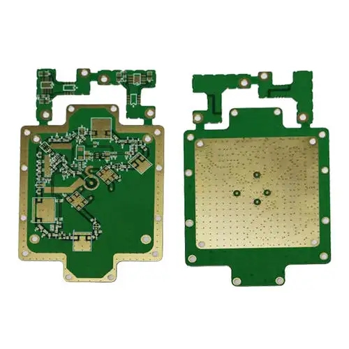
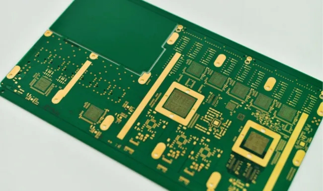
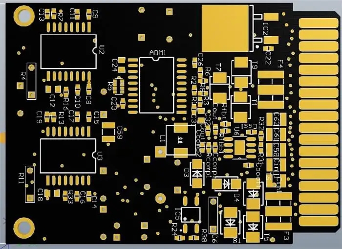
PCB制造
PCB thermal design method and design spacing requirements
PCB manufacturers, PCB designers and PCBA manufacturers explain PCB thermal design methods and design spacing requirements
In PCB production, thermal design is a very important link, whICh will directly affect the quality and performance of PCB. The purpose of thermal design is to take appropriate measures and methods to reduce the temperature of components and PCB boards, so that the system can work normally at the appropriate temperature. What are the methods of PCB thermal design?
1. Heat is dissipated through the PCB itself.
The best way to solve the heat dissipation is to improve the heat dissipation capacity of the PCB itself that directly contacts the heating elements, and to transmit or distribute through the PCB.
2. High heating device with radiator and heat conduction plate.
When there are fewer than 3 heats of a few components in the PCB, a radiator or heat conduction tube can be added to the heating components to enhance the heat dissipation effect. When there are more than 3 heating elements, a large heat dissipation cover (plate) can be used to buckle the heat dissipation cover on the element surface as a whole to contact each element for heat dissipation.
3. The main means of heat dissipation are to adopt reasonable routing design to realize heat dissipation, improve the residual rate of copper foil and increase heat conduction holes.
4. The thermal resistance between high heat dissipation devices and substrate shall be reduced as much as possible when they are connected.
5. In the horizontal direction, high-power devices are arranged as close to the edge of the printed board as possible to shorten the heat transfer path; In the vertical direction, high-power devices shall be arranged as close as possible to the top of the printed circuit board to reduce the impact of these devices on the temperature of other devices.
6. The heat dissipation of the printed circuit board in the equipment mainly depends on the air flow, so the air flow path should be studied in the design to reasonably configure the devices.
7. The devices sensitive to temperature are better placed in the area with the lowest temperature, such as the bottom of the board.
8. The hot spots shall be evenly distributed on the PCB as much as possible to maintain the uniformity and consistency of PCB surface temperature performance.
What are the spacing requirements for PCB design
When PCB engineers design PCBs, they often encounter various safety gaps. Generally, these gaps are divided into two categories: electrical safety gaps and non electrical safety gaps. What are the spacing requirements for PCB design?
1、 Electrical safety distance
1. Spacing between conductors: the minimum line spacing is also line to line, and the distance between lines and pads shall not be less than 4MIL. From the perspective of production, the bigger the better if conditions permit. Generally, 10 MIL is common.
2. Pad hole diameter and pad width: according to the situation of PCB manufacturer, if the pad hole diameter is mechanically drilLED, the minimum shall not be less than 0.2mm; If laser drilling is used, the minimum shall not be less than 4mil. The hole diameter tolerance is slightly different according to different plates, and can be controlled within 0.05mm generally; The minimum pad width shall not be less than 0.2mm.
3. Spacing between pads: According to the processing capacity of PCB manufacturers, the spacing shall not be less than 0.2MM.
4. The distance between the copper sheet and the plate edge should be no less than 0.3mm. In case of large-area copper laying, there is usually an inward distance from the plate edge, which is generally set as 20mil.
2、 Non electrical safety distance
1. Width, height and spacing of characters: For characters printed on silk screen, conventional values such as 5/30 and 6/36 MIL are generally used. Because when the text is too SMAll, the processing and printing will be blurred.
2. Distance from silk screen to pad: silk screen is not allowed to mount pad. Because if the solder pad is covered with the silk screen, the silk screen cannot be coated with tin, which affects the assembly of components. Generally, the PCB manufacturer requires to reserve a space of 8mil. If the area of some PCB boards is very close, the spacing of 4MIL is acceptable. If the silk screen accidentally covers the bonding pad during design, the PCB manufacturer will automatically eliminate the silk screen left on the bonding pad during manufacturing to ensure tin on the bonding pad.
3. 3D height and horizontal spacing on mechanical structure: When mounting components on PCB, consider whether the horizontal direction and space height will conflict with other mechanical structures. Therefore, during the design, it is necessary to fully consider the adaptability of the space structure between components, as well as between the finished PCB and the product shell, and reserve a safe space for each target object.
PCB manufacturers, PCB designers and PCBA manufacturers will explain PCB thermal design methods and design spacing requirements.


抖音二維碼

Q Q二維碼

微信二維碼
點擊
然后
聯系
然后
聯系
電話熱線
13410863085Q Q

微信

- 郵箱