鑫景福致力于滿足“快速服務,零缺陷,輔助研發”PCBA訂購單需求。


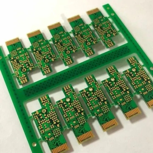
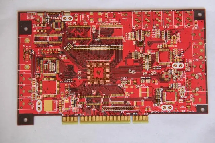
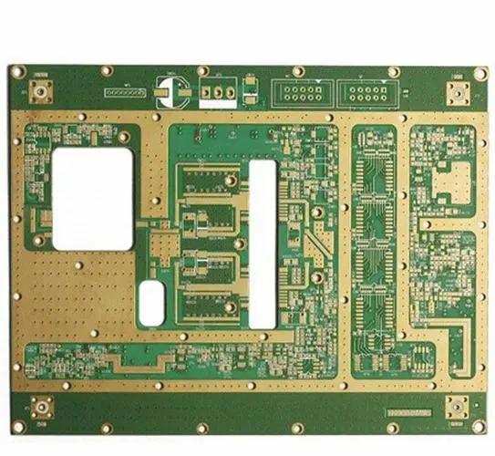
PCB制造
Measure the resistance on the circuit board and the five principles for making it
With the rapid development of electronICs and communication industries, it also promotes the continuous growth and rapid growth of PCB industry. People have increasingly high requirements for the number of layers, weight, precision, material, color, reliability, etc. of electronIC components.
However, due to the fierce MARKet price competition, the cost of PCB materials is also on the rising trend. More and more manufacturers monopolize the market at low prices in order to enhance their core competitiveness. However, the reason behind these ultra-low prices is to reduce the cost of materials and processes. However, components are often prone to cracks (cracks), scratches, (or scratches), and their precision, performance and other comprehensive factors do not meet the standards, which seriously affect the solderability and reliability of products.
In the face of various PCB boards on the market, we can start from two aspects to distinguish whether a PCB is good or bad; The first method is to judge from the appearance, and the other is to judge from the quality specification requirements of PCB itself.
Methods to judge the quality of PCB:
First, distinguish the quality of PCB from its appearance. Generally, the appearance of PCB can be analyzed and judged from three aspects;
1. Standard rules for size and thickness.
The thickness of a circuit board is different from that of a standard circuit board. Customers can measure and check according to the thickness and specification of their products.
2. Light and color.
The external circuit boards are covered with ink. The circuit board can play an insulating role. If the color of the board is not bright and there is less ink, the insulation board itself is not good.
3. Weld appearance.
Due to the large number of parts of the circuit board, if the welding is not good, the parts are easy to fall off, which seriously affects the welding quality of the circuit board. Good appearance, careful identification, and a stronger interface are very important.
Second, high-quality PCB should meet the following requirements
The telephone shall be easy to use after the components are instalLED, that is, the electrical connection shall meet the requirements;
2. The copper skin is not easy to fall off under high temperature;
3. No additional electromagnetic radiation;
4. The mechanical properties of the surface shall meet the installation requirements;
5. High temperature, high humidity and special environment resistance should also be considered;
6. The copper surface is not easy to be oxidized, which affects the installation speed. It will be damaged soon after being oxidized;
7. The line width, line thickness and line spacing of the line shall meet the requirements to avoid heating, open circuit and short circuit of the line;
8. The appearance is not deformed to avoid shell deformation and screw hole dislocation after installation. Now they are all mechanically installed. The hole position of the circuit board and the deformation error between the circuit and the design should be within the allowable range.
Five Principles of PCB process
Basis for selecting the width of printed wire: the minimum width of printed wire is related to the current flowing through the wire: if the line width of PCB is too SMAll, and the resistance of rigid printed wire is large, the voltage drop on the line will be large, which will affect the circuit performance of PCB. If the line width is too wide, the wiring density is not high, and the area of PCB increases, which is not conducive to miniaturization in addition to increasing costs If the current load is calculated by 20A/mm2, when the thickness of copper clad foil is 0.5MM, the current load of 1MM (about 40MIL) line width is 1A. Therefore, the line width of 1 – 2.54MM (40 – 100MIL) can meet the general application requirements. The line width of the ground wire and power supply on the high-power equipment board can be appropriately increased according to the power size, while on the low-power digital circuit, in order to improve the wiring density, The minimum line width is 0.254 – 1.27MM (10 – 15MIL). In the same circuit board, the power line and ground wire are thicker than the signal line.
2. The line spacing of PCB board: when the line spacing is 1.5 mm (about 60 MIL), the insulation resistance between lines is greater than 20 M Ω, and the maximum withstand voltage between lines can reach 300 V. When the line spacing is 1 mm (40 MIL), the maximum withstand voltage between lines is 200 V. Therefore, on the circuit board of medium and low voltage (the line to line voltage is not greater than 200 V), the line spacing is 1.0 – 1.5 mm (40-60 MIL). In low-voltage circuits, such as digital circuit systems, it is not necessary to consider the breakdown voltage, as long as the production process allows, it can be very small.
3. Pad: For a resistance of 1/8W, the lead diameter of the pad is 28MIL, while for a resistance of 1/2W, the lead diameter is 32MIL, the lead hole is too large, and the width of the copper ring of the pad is relatively reduced, resulting in a decrease in the adhesion of the pad. It is easy to fall off, the lead hole is too small, and it is difficult to install components.
4. Draw the circuit frame of the circuit board: the shortest distance between the frame line and the component pin pad shall not be less than 2 mm (generally 5 mm is reasonable), otherwise it is difficult to cut
5. Element layout principle:
A. General principle: In PCB design, if the circuit system has both digital circuit and analog circuit As well as large current circuits, they must be laid out separately to minimize the coupling between systems. In the same type of circuit, components must be placed in blocks and zones according to the signal flow direction and function.
B. Component placement direction: components can only be arranged in horizontal and vertical directions, otherwise they cannot be placed in plug-ins.
C. When the potential difference between elements is large, the element spacing shall be large enough to prevent discharge.
D. Input signal processing unit and output signal driving element shall be close to the circuit board edge to make input and output signal lines as short as possible to reduce input and output interference.
E. Element spacing For medium density boards, the spacing between small components, such as small power resistors, capacitors, diodes, and equal split components is related to the plug-in and welding process. During wave soldering, the component spacing can be 50-100 MIL (1.27 – 2.54 mm), which can be larger manually. For example, if 100 MIL is selected, the component spacing is generally 100 – 150 MIL for integrated circuit chips.
F. The de coupling capacitor in the IC should be close to the power supply ground wire pin of the chip, otherwise the filtering effect will become worse In the digital circuit, in order to ensure the reliable operation of the digital circuit system, the IC decoupling capacitor is placed between the power supply and the ground of each digital integrated circuit chip. The decoupling capacitor is generally a ceramIC chip capacitor, and the capacity of 0.01~0.1UF decoupling capacitor is generally selected according to the reciprocal of the system operating frequency F In addition, a 10UF capacitor and a 0.01UF ceramic chip capacitor shall be connected between the power line and the ground wire at the inlet of the circuit power supply.
G. The clock circuit component shall be close to the clock signal pin of the single chip microcomputer chip as far as possible to reduce the connection length of the clock circuit, and it is better not to run the line below.
circuit board manufacturing, circuit board design and PCBA processing manufacturers will explain the quality of resistance measurement on circuit boards and the five principles of production.


抖音二維碼

Q Q二維碼

微信二維碼
點擊
然后
聯系
然后
聯系
電話熱線
13410863085Q Q

微信

- 郵箱