鑫景福致力于滿足“快速服務(wù),零缺陷,輔助研發(fā)”PCBA訂購單需求。


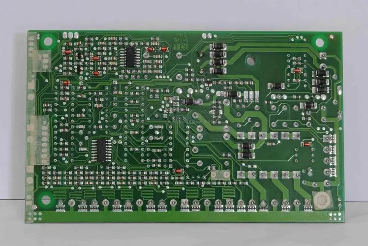
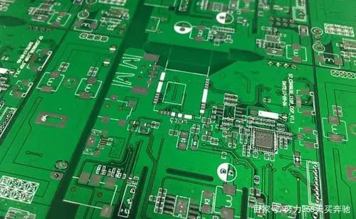
PCB制造

For pcb board manufacturers, EMC design is absolutely a key point in PCB design process. This artICle will talk about how to improve EMC from two aspects.
This paper discusses how to reduce the electromagnetic interference caused by conductive coupling and radiation coupling and improve electromagnetic compatibility from the aspects of PCB layer number design and layer layout.
1、 Introduction
Many reliability and stability problems of electronic products are caused by poor EMC design. Common problems include signal distortion, excessive signal noise, unstable signal in the working process, system crash, system vulnerability to environmental interference, poor anti-interference ability, etc. EMC design is a rather complex technology, which involves knowLEDge of electromagnetics. This paper discusses some experiential skills from the aspects of layer design and layer layout, and provides some references for electronic engineers.
2、 Configuration of layers
The layers of PCB board mainly include power layer, layer and signal layer. The number of layers is the sum of the number of layers. In the design process, the first step is to coordinate and classify all sources, places, and various signals, and deploy and design on the basis of classification. In general, different power supplies should be divided into different layers, and different grounds should have corresponding ground planes. Various special signals, such as clock high and frequency signals, need to be designed separately, and the ground plane needs to be added to shield the special signals to improve electromagnetic compatibility. When cost is also one of the factors to be considered, a balance point should be found between the electromagnetic compatibility and cost of the system in the design process.
The design of PCB power supply layer should first consider the type and quantity of power supply. If there is only one power supply, a single power layer can be considered. In the case of high requirements for power supply, multiple power supply layers can also supply power to devices in different layers. If there are multiple power supplies, you can consider designing multiple power layers, or you can divide different power supplies in the same power layer. The prEMIse of division is that there is no crossover between power supplies. If there is crossover, multiple power layers must be designed.
The design of the number of signal layers shall take into account the characteristics of all signals. The layering and shielding of special signals should be given priority. Generally, the design software is used for design first, and then modified according to specific details. Signal density and the integrity of special signals must be considered in the layer number design. For special information, the ground plane layer must be designed as the shielding layer when necessary.
Under normal circumstances, it is not recommended to design single panel or double panel if it is not purely considering cost. Although the single panel and double-sided panel are SIMple in processing and low in cost, when the signal density is relatively high and the signal structure is relatively complex, such as high-speed digital circuit or analog digital mixed circuit, because the single panel has no special reference ground layer, the loop area is increased and the radiation is enhanced. Due to the lack of effective shielding, the anti-interference ability of the system is also reduced.
3、 Layout design of PCB Board
After the signal and layer are determined, the layout of each layer also needs scientifIC design. The layout design of layers in PCB design follows the following principles:
(1) Adjacent the power plane to the corresponding ground plane. The purpose of this design is to form a coupling capacitor and work with the decoupling capacitor on the PCB board to reduce the impedance of the power plane and obtain a wider filtering effect.
(2) The selection of the reference layer is very important. Theoretically, both the power layer and the bottom plane can be used as the reference layer, but the ground plane can generally be grounded, so the shielding effect is much better than the power layer, so the ground plane is generally preferred as the reference plane.
(3) The key signals of two adjacent layers cannot cross the division area. Otherwise, a large signal loop will be formed, resulting in strong radiation and coupling.
(4) To maintain the integrity of the ground plane, it is not allowed to route on the ground plane. If the signal line density is too large, it can be considered to route on the edge of the power layer.
(5) The ground wire layer is designed below the key signals such as high-speed signal, pilot signal and high-frequency signal, so that the path of the signal loop is the shortest and the radiation is the SMAllest.
(6) How to deal with the radiation of power supply and the interference to the whole system must be considered in the process of high-speed circuit design. Generally, the area of the power plane should be smaller than that of the ground plane, so that the ground plane can shield the power supply. It is generally required that the power plane be indented twice as much as the ground plane. If you want to reduce the indentation of the power layer, you should make the thickness of the medium as small as possible.
General principles to be followed in the layout design of multilayer printed boards:
(1) The power plane shall be close to the grounding plane and designed below the grounding plane.
(2) The wiring layer shall be designed adjacent to the whole metal plane.
(3) Digital signal and analog signal shall have isolation design. First, digital signal and analog signal shall not be on the same layer. If they cannot be avoided, analog signal and digital signal can be wired in different areas, and analog signal area and digital signal area can be separated by slotting. The same is true for analog and digital power supplies. In particular, the digital power supply has very large radiation, so it must be isolated and shielded.
(4) The printed line in the middle layer forms a planar waveguide and the microstrip line in the surface layer. The transmission characteristics of the two are different.
(5) Clock circuit and high-frequency circuit are the main interference and radiation sources, which must be arranged separately and away from sensitive circuits.
(6) Stray current and high-frequency radiation current contained in different layers are different, so wiring cannot be treated equally.
The electromagnetic compatibility of PCB can be greatly improved through the layer number design and layer layout.
The number of layers shall mainly consider the power supply layer and ground wire layer, high-frequency signal, special signal and sensitive signal.
PCB layout mainly considers various coupling, ground wire and power line layout, clock and high-speed signal layout, analog signal and digital information layout.


抖音二維碼

Q Q二維碼

微信二維碼
點擊
然后
聯(lián)系
然后
聯(lián)系
電話熱線
13410863085Q Q

微信

- 郵箱