鑫景福致力于滿足“快速服務(wù),零缺陷,輔助研發(fā)”PCBA訂購(gòu)單需求。


行業(yè)新聞

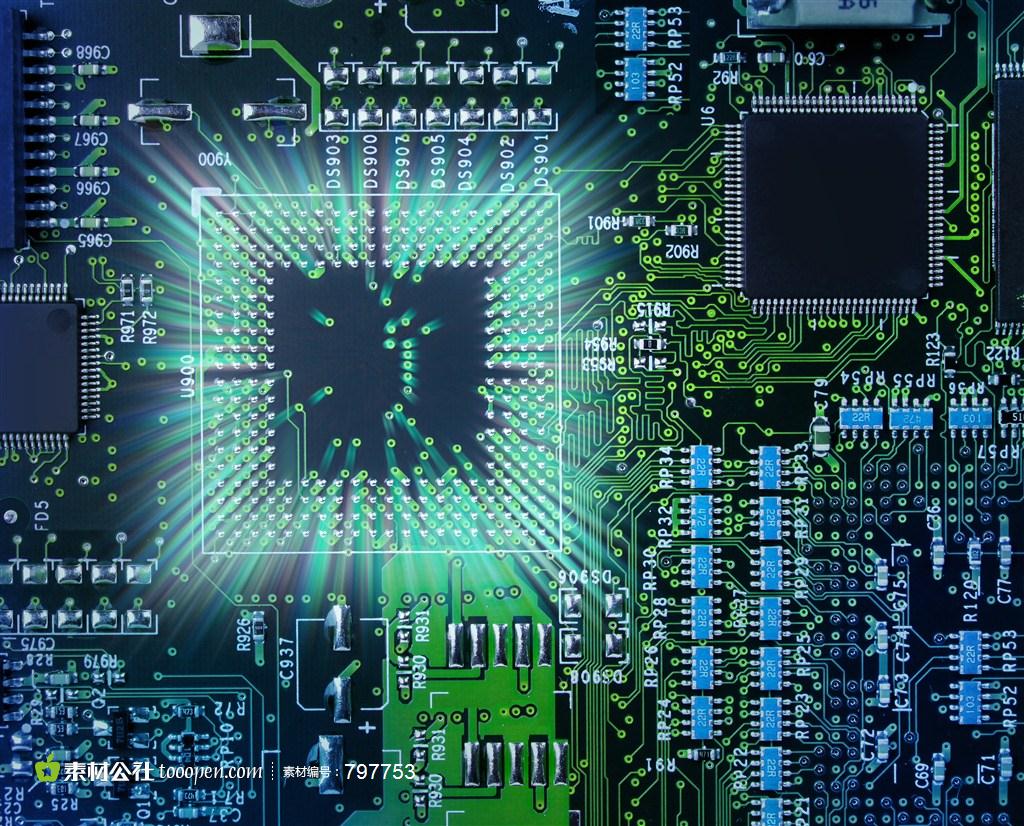
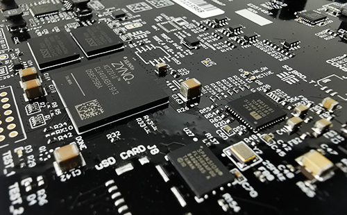
PCB board design and signal integrity analysis
1.. Signal integrity analysis
Factors related to SI: reflections, crosstalk, radiation Reflection is caused by impedance miSMAtch on transmission path; Crosstalk is caused by line spacing; Radiation and high-speed equipment itself and PCB design
Transmission line judgment
Using the previous formula for judging high speed signals
Judgment steps:
1) Obtain the effective frequency Fknee of the signal and the trace length L;
2.) Use Fknee to calculate the effective wavelength ? knee of the signal, that is, ? knee=C/Fknee;
3.) Judging the relationship between L and 1/6x ? knee, if L>1/6x ? knee, the signal is a high-speed signal, otherwise it is a low-speed signal; Where knee=C/F knee; Where, C is the speed slightly lower than the speed of light, and F inflection point=0.5./Tr (10%~90%). It should also be noted that if there is no ready board for 100M frequency signal, the effective frequency Fknee, and Fknee is about 7 tiMES the Fclock (signal period) can be estimated If L>1/6x ? ? knee, it is regarded as a transmission line, and the reflection of signal must be considered for the transmission line, whICh may be caused by impedance mismatch during transmission Reflection formula: signal reflection ? ?= (Z2-Z1)/(Z2+Z1); where Z2 is the line impedance after the reflection point; Z1 is the line impedance before the reflection; The possible value of The reflection of the signal is caused by the origin impedance mismatch, transmission path, and termination Method of reducing reflection: In order to reduce the reflection of signal as much as possible, Z2 and Z1 need to be as close as possible There are several methods for impedance matching: series matching at the sending end, parallel matching at the receiving end, voltage division matching at the receiving end, parallel matching of resistance and capacitance at the receiving end, and parallel matching of DIPoles at the receiving end
4) Receiver voltage divider matching
5) Parallel matching of resistance and capacitance at the receiving end
Advantages: less power consumption;
Disadvantage: There is a mismatch between the high and low levels of the receiving end. Because of the capacitor, the edge change of the signal will slow down

2. Signal circuit
The signal loop mainly includes two paths The signal level measured at the sending end, the transmission path and the receiving end are essentially signal voltages at corresponding positions on the drive path and return path Value, these two paths are very important The following points need to be noted:
1) When the signal layer is changed, do not change the reference layer If the signal is changed from signal layer 1 to signal layer 2, the reference layer is the bottom layer 1. In this case, the return path does not need to change the layer, that is, the signal change layer has no effect on its return path
2) When the signal changes layers, the network content of the reference layer remains unchanged That is, the reference layer at the beginning of signal 1 is power layer 1/bottom layer 1. After changing the layer, the reference layer of signal 1 is power layer 2/bottom layer 2. The network content of the reference layer remains unchanged, all of which are GND or power content The return path can be wired using the nearby GND or power via Here, at high speed, the capacitive reactance and inductive reactance of the via cannot be ignored In this case, the vias should be minimized to reduce the impact of impedance changes caused by the vias themselves and reduce the impact on the signal return path
3) When the signal layer is changed, add a through-hole with the same content as the reference layer near the signal through-hole
4) If the network properties of the two reference layers are different before and after the layer change
5) When the signals of changing layers are deny, a certain distance should be kept between the nearby ground or power holes When there are many layers of varying signals, it is necessary to set more through holes on the ground or power supply
3. Crosstalk
The solution to crosstalk is that high speed signals PCB, clock signals, other data signals, etc, The spacing shall meet the 3W principle
The above is the explanation given by the editor of PCB circuit board company. If you want to know more about PCBA, you can go to our company's home page to learn about it. In addition, our company also sells various circuit boards,
High Frequency Circuit Board and SMT chip are waiting for your presence again.


抖音二維碼

Q Q二維碼

微信二維碼
點(diǎn)擊
然后
聯(lián)系
然后
聯(lián)系
電話熱線
13410863085Q Q

微信

- 郵箱