鑫景福致力于滿足“快速服務,零缺陷,輔助研發”PCBA訂購單需求。


行業新聞
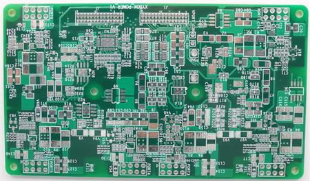
There is a limit to how many circuits can be instalLED on a board. For the reason of manufacturing equipment and standard panel size, PCB itself has a size upper limit. The number of transistors on a devICe continues to expand, while resistors and capacitors almost disappear to the naked eye. Even if all the integration and miniaturization, the complexity of the circuit will also grow to a scale that is difficult to manage. One PCB does not solve the problem.
There are many expansion forms beyond a single PCB. Telecommunications and other network equipment often appear in rack systems. The familiar 19 inch wide x 1.75 inch high rack unit is the default enclosure size for SMAller circuits. This is what you see when you read the term server farm or data center. From there, the baseline extends to multiple rack units. Although they are available in various sizes, seven rack shelves are popular. It is still 19 inches wide, but it takes just over a foot of rack space. The rack is equipped with vertically placed PCBs and connected with a 19 "x 12" backplane, which is installed on the back of the rack.
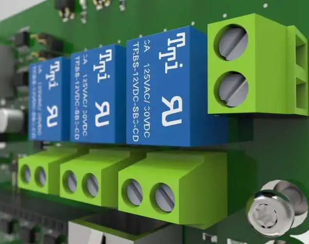
The backplane is usually just a connector and PCB wiring. The number of layers may be high to support a large number of connections. The thickness of this plate provides the stiffness required to engage the 640 pin connector while resisting anyone attempting to preheat the backplane before welding. Therefore, press fit connectors are standard on these types of printed circuit boards.
Handling thick plates
In addition to PCB connectors, we usually need some sort of housekeeping circuit. These components will need to be surface mounted, especially when the backplane is on the thicker side. The standard pins on the through-hole components do not reach the required length at the far end of the backplane, so they are not solderable or reworkable. Then there is the aforementioned pound copper for the grounding plane to increase the return temperature. clumsily.
Another consideration related to thickness is the through hole in the Z-axis. If wiring from the top to the fourth layer of the 24 layer board, the other 20 layers will form suspension wires. This discontinuity can be eliminated if we return after all electroplating and drill a new slightly larger hole at the location of 20 layers of short piles. Reverse drilling requires extra effort, but the results on the signal integrity eye map can be measured.
This brings us to all other PCBs in the system. In the data center, server blades will occupy most of the slots, so you can expect some uniformity. The system has scalability, and each new board can improve the overall performance.
Other network devices may be more diversified. Each card slot has a different purpose, and each card slot must be populated for the entire group to function properly. Because of all the huge parts and the consequent extreme voltage swing, the power supply is usually a separate board. The most power consuming card finds a place next to the power supply, while the most sensitive victim hides in his own small box away from heat and noise. Think of all the gadgets that come down from the wall warts. The power supply is placed on the power socket and the juice is conveyed to the rest of the system through ferrite beads and/or shielded wires. The same principle.
Good neighbourliness policy
The subdivision of the remaining schematIC parts into circuit boards is usually based on block diagrams. How these modules are combined should depend on the technology involved. Some circuits will require higher layers or active HDI technology. Others can live with four layers of vanilla. Fine adjustment in function and technology depends on power range, coexistence, thermal path, weight distribution and final aesthetics. I remember that a board in a system is called "tROtS board". Stands for "the rest of the story". SometiMES, another word will replace "story".
Not all systems require a 7-foot rack with electronics to qualify. Only a few PCIe or SATA connectors are required. The example I think of is the prototype version of Google's "home" mesh router. With another Qualcomm chipset, this is a larger size. Three additional PCIe card slots enable it to test the functionality of multiple router configurations. Air interface is another thing. The only real way to test the wireless part of the link is to establish a test room. We used a four board system to enable baseband level testing in the laboratory. Prototypes are one of the cool things you've heard about 20% of the time.
These micro systems may give you more freedom. In general, the backplane is more a motherboard that carries some computing loads. In this case, the suspect you usually need must attend the meeting. Memory and various drivers may find houses next to microprocessors. Of course, the memory usually resides on the SIM module, which comes down to a circuit board with a connector and a row of memory chips. In this respect, it can be considered as another board of the system. Any indicator lights, buttons, displays or other controls used in the product will eventually appear on this PCB layout.


抖音二維碼

Q Q二維碼

微信二維碼
點擊
然后
聯系
然后
聯系
電話熱線
13410863085Q Q

微信

- 郵箱