鑫景福致力于滿足“快速服務,零缺陷,輔助研發”PCBA訂購單需求。


行業新聞

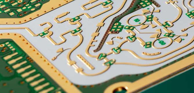
Some SMPS PCB layout tips and noise and thermal problems
p> Whether AC-DC or DC-DC conversion PCB board is implemented, switching power supply layout is very common in high-voltage design, and must be carefully constructed Although this kind of system is very common, it is easy to generate radiated EMI due to the rapid change of voltage and current during switching Designers are rarely able to adapt existing designs to new systems because SMAll changes in an area can create EMI problems that are diffICult to diagnose Proper layout, selection and routing can prevent noise from becoming an important issue in SMPS output Low voltage converters can be purchased as ICs with different shape factors, but high voltage converters will need to be produced by discrete components on special circuit boards Here are some important SMPs: PCB layout tips can help you keep components cool and prevent noise problems in the system
Noise and Thermal Issues in SMPS PCB board layout
There is no fix: any SMPS will generate moderate high frequency noise due to the switching action of the transistor driver. In fact, you are converting low frequency rip (i.e. from a full wave receiver during AC-DC conversion) into high frequency switching noise Although this conversion produces a more stable DC output, there are still two important noise sources: direct switching noise from switching elements Transient noise elsewhere in the system Noise may appear at the output of SMPS unit in the form of conduction and radiation noise Although the cause of each problem is difficult to diagnose, it is easy to distinguish between two types of noise Another design challenge for SMPS is the heat generated on the PCB layout This can affect the duty cycle and rise time by selecting the correct PWM frequency. You still need to use the correct thermal management strategy on the board Considering these two challenges, let's take a look at some details of PCB layout in SMPS
thermal management
An ideal SMPS would disperse zero power, although in practice, this did not happen Your switching transistors (and the input transformer for AC-DC conversion) will dissipate most of the heat. Even though the efficiency can reach 90% in the switching power supply topology, power MOSFETs can still emit a lot of heat during switching The common practice here is to place the radiator on the key switch assembly Make sure they are reconnected to the ground plane to prevent new EMI High voltage/high current power supply, these radiators may be quite large You can increase the cooling capacity of the system by installing a fan on the main chassis Once again, ensure that good practices for powering fans are followed to prevent new EMI problems
Some SMPS PCB layout tips
Your layout will help with thermal management to some extent Typically, conducted noise is handLED by using EMI filters on input and output circuits Like many EMI problems at high speed/high frequency systems, your stack will be the main determinant of radiation EMI resistance The relevant frequency range of switching power supply operation is~10kHz~1MHz, and the radiated EMI will cause induced noise Therefore, the ground plane is placed directly in the stack below the surface layer, as well as all power components This will ensure a low loop inductance in the surface circuit Any induced noise transmitted to the output is usually eliminated by filtering at the output
transient ringing
Transients are a more difficult problem to solve because they are related to your stack As the case in high-speed design, do not wire any copper carrying switch signal to the gap of the grounding plane, because this creates some type of antenna structure, and the radiation is strong during the transient These transients tend to be high frequency (anywhere from 10 to 100 MHz). The transient ringing problem is an impedance management problem High impedance leads to strong voltage ripple Components should be placed in the correct pad pattern to minimize impedance in the circuit board PDN Examples of good pads and bad pads for components are shown below
The quality of the components in the layout
In general, do not keep any islands in the layout Use decoupling capacitors to connect any power island that may contain control circuits or passive components back to the ground/ground plane In this case, place any through hole PCB board carefully because you do not want to create unexpected gaps or sockets in the ground plane
The above is the explanation given by the editor of pcb circuit board company. If you want to know more about PCBA, you can go to our company's home page to learn about it. In addition, our company also sells various circuit boards,
High Frequency Circuit Board and SMT chip are waiting for your presence again.


抖音二維碼

Q Q二維碼

微信二維碼
點擊
然后
聯系
然后
聯系
電話熱線
13410863085Q Q

微信

- 郵箱