鑫景福致力于滿足“快速服務,零缺陷,輔助研發”PCBA訂購單需求。


行業新聞
PCB layout analog circuit and digital circuit
The placement direction of PCB components determines the direction of wiring
2. The wiring direction of adjacent layers is different, and the wiring body of the surface layer and solder layer of the two panels is 90 degrees
3. The wiring direction of rectangular circuit board is vertICal, and horizontal wiring is easy to lead to blockage or even impossible wiring.
4. Try to ensure the wiring space. If this is not possible, use the wiring below a specific component to avoid setting connection holes below the component.
Because when the circuit board fails, it is impossible to visually see the status of the connection hole under the component and whether it is short circuited with other wiring or component pins.
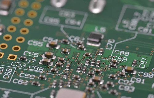
PCB board

Analog circuit part and digital circuit part
Including wiring, analog circuit and digital circuit shall be kept above 5mm to ensure no signal interference between them. When symbols are used to represent the grounding wire in the circuit diagram, the circuit board designer needs to analyze the circuit diagram and set the setting area. Power and ground wires Power and ground wires were originally designed. For the two panels and the four layer board, the wiring composition is completely different, because the power cord and ground wire are set in the inner layer and are mainly concerned. Only focus on the layout of signal lines. For beginners, it is recommended to learn the design of four layer boards. The wiring of power lines and ground wires has a great impact on power and clutter, and this should be carefully designed.
Take two panels for example:
1) The power line and ground wire are designed on the same floor, and the effect is poor
2) The ground wire is on the surface layer and the power wire is on the welding layer. Overall design
3) The grounding wire is on the surface layer, the power line is on the welding layer, and the copper foil is used for wiring. The anti clutter effect is better. Due to the uncontrollability of CAD design, the design time is longer than that of SIMple wiring. Take care to ensure that the wiring width is SMAll to ensure that there are no breaks and blockages.
Simply put, the power cord and ground wire are equivalent to the human aorta and vein. You can also simply think of it as a water pipe. The wider the line width, the greater the current that can pass through, and the faster the heat dissipation. The narrower the line width, the greater the resistance under the same voltage, the smaller the current that can pass through, and the slower the heat dissipation.
Welding surface
For power line and ground wire, use large area copper foil wiring. Precautions for power and ground wiring of double-layer circuit board. Generally, the power line is wired on the welding surface, the ground wire is wired on the surface, copper foil is used for wide area wiring, and then some capacitors are added between the power line and the ground wire, which is basically no problem. But when it coMES to electromagnetic interference, the problem is different. When it exceeds 8MHz, problems of one kind or another may occur. When it exceeds 25MHz, it will be very unstable. At this time, it is necessary to surround the ground wire copper foil around the important parts and design the ground wire copper foil on the welding surface.
Wiring of crystal oscillator
In order to resist interference, surrounding parts shall be surrounded by ground wire copper foil as much as possible. What is not shown in the figure is that the copper foil of the grounding wire can also be placed under the crystal oscillator of the solder layer, and then connect the surface and the solder surface through the connection hole. Enhance anti-interference capability.
Use of heat pad
When bulk copper foil is used for power and ground wiring, heat resistant pads should be designed as far as possible. This is because if the component pad is directly connected to a large piece of copper foil, the heat will dissipate rapidly during welding, and the temperature of melted solder is not enough, resulting in poor welding or virtual welding.
Heat pad
Power supply of analog circuit: the output part shall be close to the power supply, and the high sensitivity input part shall be separated from the output part by a certain distance, so as not to be affected by the output part DC power supply: when the power is supplied from the outside, it must first pass through the electrolytic capacitor and then be supplied to the internal circuit The wiring method is generally as follows: Double panel, not through point A, but through point B, supplies power to internal circuits After passing point B, the multilayer PCB also inputs power to the inner layer
The above is the explanation given by the editor of PCB circuit board company. If you want to know more about PCBA, you can go to our company's home page to learn about it. In addition, our company also sells various circuit boards,
High Frequency Circuit Board and SMT chip are waiting for your presence again.


抖音二維碼

Q Q二維碼

微信二維碼
點擊
然后
聯系
然后
聯系
電話熱線
13410863085Q Q

微信

- 郵箱