鑫景福致力于滿足“快速服務,零缺陷,輔助研發”PCBA訂購單需求。


行業新聞

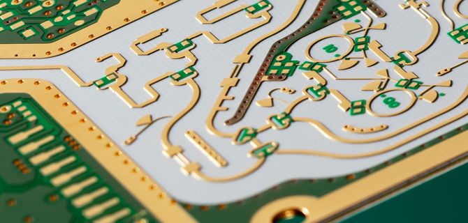
14 Common Errors in PCB Design for Engineers
1. Overlap of pads
1) The overlaying of the pads (except the surface mount pads) means that the holes are overlapped
2) The two holes in the middle overlap. For example, one hole is an isolation disk, and the other hole is a connection disk (flower pad). The negative pole is drawn as an isolation disk, resulting in scrapping.
2. Abuse of layers
1) Some useless connections have been made on some graphIC layers, but at first more than five layers of circuits were designed, which caused misunderstanding.
2) Setting up maps is easy. Take Prol software as an example, use board layer to draw lines on each layer, and use Board layer to MARK lines. In this way, when light drawing data is executed, the connection will be lost because no slab is selected. Line, or because the dimension line of the slab layer is selected, the graphic layer is kept complete and clear in the design process.
3) It violates the conventional design, such as the surface design of the component is at the bottom and the surface design is at the top, causing inconvenience.
PCB board

3. Random placement of characters
1) The SMD solder label of the character covering pad brings inconvenience to the on-off test of the printed circuit board and the welding of the components.
2) If the character design is too SMAll, it will make screen printing difficult. If it is too large, the characters will overlap each other, making it difficult to distinguish.
4. Setting of single pad aperture
1) Single sided gaskets are usually not drilLED. If it is necessary to mark the hole, the hole diameter shall be designed as zero. If this value is designed so that the coordinates of the hole appear at this position when generating drilling data, a problem occurs.
2) Single sided pads, such as drilled holes, shall be specially marked.
5. Use filler blocks to draw pads
The drawing pad with filler block can pass DRC inspection during circuit design, but it is not suitable for processing. Therefore, it cannot be directly used to generate welding mask data. It is difficult to solder devices.
6. The electric layer is both a flower pad and a connection
Because the power supply is designed in the form of flower pads, the grounding plane is opposite to the image on the actual PCB, and all connections are isolation lines. The designer should be very clear about this. Here, by the way, be careful when drawing multiple groups of power or grounding isolation lines to avoid leaving gaps, short circuiting two groups of power supplies, or sealing the connection area (thus separating one group of power supplies).
7. Unclear definition of processing level
1) The single panel design is on the top floor. If the front and back sides are not specified, it may be difficult to weld the fabricated plates of the installed equipment.
2) For example, the four layer board is designed as the top mid1 and bottom mid2 four layers, but it is not placed in this order during processing, which needs to be explained.
8. Too many filler blocks in the design, or extremely thin lines filled with filler blocks
1) The generated light rendering data is lost, and the light rendering data is incomplete.
2) Since fill blocks are drawn one by one during photo data processing, the amount of photo data generated is quite large, which increases the difficulty of data processing.
9. The pad of surface mounted device is too short
This is for switch testing. For surface mounted equipment with excessive density, the distance between two feet is very small and the pad is very thin. When installing test pins, they must be staggered up and down (left and right), such as pads. If the design is too short, although it will not affect the installation of the equipment, the test pin will be in the wrong position.
10. Large area grid spacing is too small
The edge between the same lines forming a large area grid is too small (less than 0.3mm), and during the process of the printed circuit board, after the completion of the image transfer process, many damaged films are likely to adhere to the circuit board, resulting in wire breakage.
11. Large area copper foil is too close to the outer frame
The large area of copper foil shall be at least 0.2mm away from the outer frame, because when milling the shape, if the copper foil is milled, it is easy to cause the copper foil to bend and the solder is not easy to fall off.
12. Uneven plane design
In the process of pattern electroplating, the coating is uneven, which affects the quality.
13. When the copper area is too large, use grid lines to avoid PCB
The above is the explanation given by the editor of pcb circuit board company. If you want to know more about PCBA, you can go to our company's home page to learn about it. In addition, our company also sells various circuit boards,
High Frequency Circuit Board and SMT chip are waiting for your presence again.


抖音二維碼

Q Q二維碼

微信二維碼
點擊
然后
聯系
然后
聯系
電話熱線
13410863085Q Q

微信

- 郵箱