鑫景福致力于滿足“快速服務,零缺陷,輔助研發”PCBA訂購單需求。


行業新聞

AOI Exploration of 6 Sigma PCBA Assembly
How to check assembly defects in modern inspection system, analyze the root cause of PCBA component defects, and explore the 6Sigma of measurement system
1 Introduction
How did assembly defects occur? Why do some PCBA components produced by the assembly line meet the requirements, while other components are endlessly reworked due to multiple assembly errors? Why does the assembly quality vary from batch to batch? More importantly, what experience should we gain from these changes, and what should we do to exclude changes in PCBA assembly. The above problem is the traceability of 6 Sigma production. Sigma is a Greek letter that describes the distribution or dispersion of the average value of any process parameter, that is, the standard deviation. Six Sigma uses statistICal techniques to determine the process state by measuring the process capability, and then finds out the main variables that affect the process capability through comparative analysis, and uses process optimization methods to find out the change rules, and then eliminate them. Or control, improve the control loop through continuous measurement and analysis, continuously improve the process capability, and finally reach or exceed the 6 Sigma level.
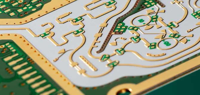
PCB board

2.6 Sigma and PCBA assembly
Variability refers to any change that has a potential negative impact on product quality pcb board design shall comprehensively consider the reliability of its electrical and mechanical efficiency, such as component pad design tolerance, pad pattern design, etc Secondly, the size and quality of the components and data used to assemble PCBA will also affect the assembly quality, Changes in the assembly process itself will also affect the quality of PCBA components In the PCBA module, the mutation is the "enemy" After eliminating the obvious sources of differences in design and data, the remaining parts are variations of the PCBA process itself, using PCB boards, components, solder pastes, etc The content data indicates an accident and fixes the defects caused by process changes. The content data is usually positive/negative, good/unpleasant, I/O type data Variable data records the degree of process change, which is not directly expressed as defects, but digital data, measurement type, etc Must record and relate to content data, unexpected defects, or the probability of defects occurring Content data checking is a way to observe whether there are unacceptable changes The characteristics and frequency of content data are related to the source of variation Defects are usually found during circuit testing, functional testing, automatic optical image analysis or manual visual inspection, or other methods for checking PCBA Some changes in the PCBA manufacturing process are inevitable, and measures should be taken in advance to prevent such situations, which is calLED "acceptable process change" APV is usually the tolerance of the assembly process or acceptable mechanical differences in components, raw materials, etc APV generates variable data, but it will not be the source of defects in the final product If APV has undoubted defects or repaired defects, design or manufacturing problems must be improved in advance Unacceptable process change refers to the change that has not been detected and will inevitably lead to defects or high probability of defects Jinli's process shall accept APV, detect and reject UPV Six Sigma is used to define the method and necessary error for distinguishing APV and UPV In order to identify changes and provide continuous measurement of changes and defects, we must understand various data and content data when actually producing PCBA In order to implement measurement, it is necessary to understand the measurement mechanism of measurement variable data and content data in PCBA production Content data testing is the key to inspection and testing in the production of polychlorinated biphenyls Modern PCBA component factories are usually equipped with modern detection systems, such as automatic optical image analysis, online testers, and functional testers to scan and detect defects, and send the inspection results to the operator
3. Main Sources of Electronic Product Assembly Defects
Because all variations can lead to defects, variation is the "enemy" of production. Combined with PCBA production process, we mainly discuss the source of defects in SMT production. In combination with the main processes of solder paste printing, repair welding and reflow soldering, the discussion is as follows:
Solder paste printing: error (problem): solder paste printing missing, solder paste short circuit, solder paste pollution. Difference (change): solder paste coverage area, solder paste coverage height, solder paste coverage volume, solder paste coverage pattern. Inspection: Solder paste coverage/missing, adjacent pads inspection, solder paste coverage area inspection. Measurement: Solder paste coverage area, solder paste coverage height, solder paste coverage volume, solder paste coverage pattern. SMD: Error (problem): missing element, wrong element direction, damaged element, wrong element. Differential occlusion): x-Y-z axis, part/pad registration, assembly registration. Check: pasted/missing pasted components, component direction signs/MARKs, component packaging shape. Measurement: x-y-z axis, part/pad alignment, assembly alignment. Reflow fault (problem): component placement characteristics, component installation, tombstone phenomenon, weld bead, solder short circuit, etc. Check all wing lead solders, all J lead solders, solder short circuit check, check discrete components (floating), random contamination of components, etc.
4. Automatic optical image detection
During the assembly process, the solder paste amount and solder joint shape of sEMI-finished products, the thickness of bare circuit board wires and the defects of wires should be continuously checked, which are usually undetectable by online testing or functional testing. Visual inspection has many errors and low efficiency. Automatic optical image inspection is recognized as an effective method. At present, optical image automatic detection adopts two methods: design rule detection and pattern recognition. The design rule inspection method is to check the circuit pattern according to two given rules. For example, all connections should be terminated with solder joints, the width of all leads should not be less than 0.127 mm, and the spacing between all leads should not be less than 0.102 mm. This method can ensure the correctness of the circuit under test from the calculation. Pattern recognition is to compare the stored digital image with the actual work. The inspection shall be conducted according to the inspection file created by the well inspected printed circuit board or glass model, or according to the inspection program prepared in the computer aided design. The accuracy depends on the resolution and the checking program used. The modern automatic optical image detection system can ensure the measurement and tracking of extremely SMAll x, Y, F (rotation) position deviation changes when detecting the placement characteristics of the elements. The inspection process is very sensitive, measuring some changes that should be eliminated, such as position, size and image, and recording some acceptable process changes, such as component supplier change, nominal size, logo or default color (allowed), as well as the location characteristics of the component placement process.
5. Research and development of optical image automatic detection system
The repeatability of measurement results refers to the consistency between the results obtained from continuous and multiple measurements of the same object under the same measurement conditions. The reproducibility of measurement results refers to the consistency between measurement results of the same measured object under changing measurement conditions. For modern AOI systems, the repeatability of measurement results is very important. Because key changes can be identified through the AOI system, but to draw accurate conclusions on the change trend, the AOI system needs to have good measurement repeatability to distinguish between process changes and changes in the measurement system itself. According to the requirements for the number of testing capacity, the selection of standard devices generally follows the principle of 1/3, that is, the ratio of the accuracy of the standard device to the accuracy of the measured instrument should be kept at 1/3. In the part inspection of the mechanical industry, the ratio of measurement limit error to tolerance is called the precision coefficient, which should generally be kept within the range of 1/3 to 1/10. The detailed calculation of measurement uncertainty (RaR) of AOI system is not listed here. The measurement uncertainty of the modern AOI system is better than ± 0.4mil when the confidence factor is 3, which means that 99.73% of the measured values are within the upper and lower specification limits. Actually
In the production of Sigma PCBA, what is the measurement uncertainty required by AOI system? It is generally believed that the current SMD component size is 0201. If 50% deviation from the gasket needs to be detected, the required measurement value is 0.127mm. Using the 1/10 principle of the above AOI measurement system, when the confidence factor is 3, the measurement uncertainty of the AOI measurement system is less than 0.0127mm. For the current QFP package IC, its size is 0.4064mm ? 0.2032mm, the detection requirement is also 50% of pad, that is, when the confidence factor is 3, the measurement uncertainty of AoI measurement system is required to be less than 0.01016mm. The above 6Sigma PCBA test means that the change of ± 3 Sigma from the center of the specification value is considered as "normal or acceptable" change.
7. Ability to measure patches (pick and place)
In SMD process inspection, how to select inspection standards to ensure the repeatability of the six SIGMA? The following are QFP0402 components, with repeatability of ± 0.0508mm (confidence factor of 3) and spacing of 0.0508mm, based on SMD process capability. Take 50% of pads as an example of SMD process inspection required for inspection: first, develop an average value to determine the distribution of measurement results of process statistics σ At the confidence factor, the repeatability of SMD placement is ± 0.0508mm. And the distribution drift of the average value with time, temperature and maintenance cycle. This specification is part of the inherent characteristics of the equipment and its source is very important. If this is a device function, users need to reconsider. Whether this feature represents the comprehensive features of SMD process delivery, picking and placement, including changes in SMD component size, PCB supplier, PCB deformation, etc. It needs to be decomposed into the characteristics of the equipment actually delivered, or test a series of products under different time and temperature conditions, and calculate the distribution drift of different batches of samples. Secondly, we must realize that the 50% off ground inspection requirement is the limit of the pick and place inspection application in the SMD process, and many products actually specify a tolerance of 30% or less. Third, the deviation between components and gaskets shall be calculated as 50%. For 0402QFP parts, the 50% deviation from the gasket represents a deviation of 0.127mm. Recall that the measurement uncertainty of the AOI measurement system shall be less than 0.0127mm when conducting AOI inspection. It can be calculated that when the confidence factor is 3, for the process distribution of ± 2mils, 50% deviation from pad is used as the detection requirement, representing 7 σ Placement detection limit (assuming that the average distribution remains stable).
8. Conclusion
Six Sigma PCBA production will be our goal The combination of 6 Sigma and modern automatic optical image detection equipment has significantly reduced the total number of PCBA components. It has been proved that there are errors During component placement, it can provide accurate and repeatable position measurement to confirm its 6 Sigam effectiveness Automatic optical image detection is essential to ensure the effectiveness of 6 Sigam The third generation of modern automatic optical image detection system, its repeatability, performance and speed can meet the requirements of modern PCBA components At the same time, it provides the manufacturer with the key measurement values in the assembly process, and combines the inspection statistical results with the repair process to provide a comprehensive closed-loop control to ensure product quality PCBA component production


抖音二維碼

Q Q二維碼

微信二維碼
點擊
然后
聯系
然后
聯系
電話熱線
13410863085Q Q

微信

- 郵箱