鑫景福致力于滿足“快速服務,零缺陷,輔助研發”PCBA訂購單需求。


行業新聞

design specifICation for PCB board in switch voltage regulator production
In the design and production of power supply, the design and production of PCB is very important In any switching power supply design, the physical design PCB is a link If the design method is not appropriate, this PCB may cause many problems Based on many years' experience in PCB design, especially in power supply design and production, the author analyzes the precautions in each step
Design process
The design process from drawing to PCB board is: establish component parameters – input principle net list – design parameter setting – manual layout – manual routing – verify design – review – CAM output.
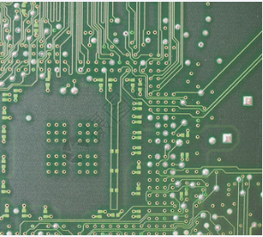
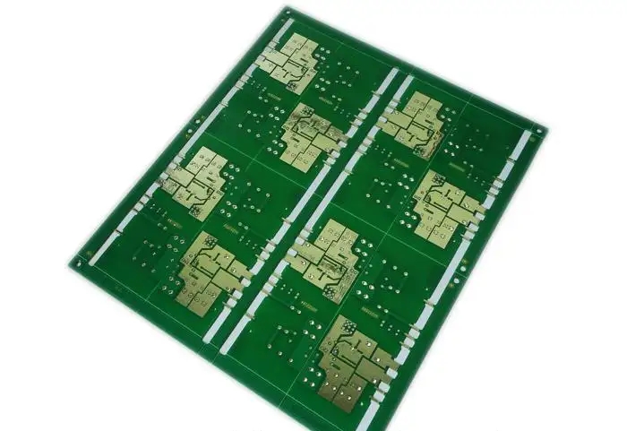
PCB board

Electrical safety requirements
The spacing of wires must meet the electrical safety requirements, and the spacing must at least be suitable for withstand voltage. In order to facilitate operation and production, the spacing should be as wide as possible. When the wiring density is low, the spacing of signal lines can be appropriately increased. For signal lines with high level and low level differences, the spacing shall be increased as much as possible, generally 8mil. The distance from the inner hole edge of the pad to the edge of the printed board shall be greater than 1mm to avoid pad defects during processing. When the trace connected to the pad is thin, the connection between the pad and the trace should be designed as a water drop shape, which has the advantage that the pad is not easy to peel off, and the trace and the pad are not easy to disconnect.
Component Layout
The component layout practice has proved that even if the circuit schematic is correctly designed and the printed circuit board is improperly designed, the reliability of electronic equipment will be adversely affected. For example, if two thin parallel lines on the PCB are close together, the signal waveform will be delayed, thus generating reflective noise at the end of the transmission line. This, when designing the printed circuit board, pay attention to the correct method. The switching power supply has four current circuits: power switch AC circuit, output rectifier AC circuit, input signal source current circuit and output load current circuit. The input circuit uses approximate DC current to charge the input capacitor, and the filter capacitor is mainly used for broadband energy storage; SIMilarly, the output filter capacitor is also used to store high-frequency energy from the output rectifier and eliminate the DC energy of the output load circuit. In this case, the input and output current circuits should only be connected to the power supply from the filter capacitor terminals; If the connection between the input/output circuit and the power switch/rectifier circuit cannot be directly connected to the capacitor terminals, AC energy will pass through the input or output. Filter the capacitor and radiate it to the environment. The AC circuit of the power switch and the AC circuit of the rectifier contain high amplitude ladder current. These currents have higher harmonic content and their frequencies are much higher than the switching fundamental frequency. The peak amplitude can be up to 5 tiMES the amplitude of continuous input/output DC current. The transition time is usually about 50ns. These two circuits are vulnerable to electromagnetic interference. These AC circuits must be wired before other tracks in the power supply. Filter capacitors, power switches or rectifiers, inductors or transformers of each circuit shall be placed adjacent so that the current path between them is as short as possible.
The following principles shall be followed when arranging all components of the circuit:
1) When the PCB board size is too large, the printed circuit will be very long, the impedance will increase, the noise resistance will be reduced, and the cost will also increase; If it is too SMAll, the heat dissipation will be poor and adjacent lines will be vulnerable to interference. The shape of the circuit board is rectangular, and the aspect ratio is 3:2 or 4:3. The distance between the components at the edge of the circuit board and the edge of the circuit board is usually not less than 2mm.
2) When placing the equipment, consider the subsequent welding, not too intensive.
3) The layout is centered on the components of each functional circuit. The components shall be uniformly, orderly and compactly arranged on the PCB to minimize and shorten the leads and connections between components. The decoupling capacitor shall be as close to the VCC of the components as possible.
4) For circuits operating at high frequency, the distribution parameters between components shall be considered. In general circuits, elements shall be arranged in parallel as far as possible. In this way, it is not only beautiful, but also easy to install, weld and mass produce.
5) Arrange the position of each functional circuit unit according to the circuit process, so that the layout is convenient for signal flow and the signal transmission direction is as consistent as possible.
6) The first principle of layout is to ensure the wiring rate of wiring. Pay attention to the connection of flying wires when moving devices, and put the devices with connection relationships together.
7) Reduce the loop area as much as possible to suppress the radiated interference of switching power supply.
High frequency processing
The length and width of a conductor affect its impedance and inductance, and thus its frequency response. Even traces passing through DC signals may be coupLED with RF signals of adjacent traces and cause circuit problems (or even radiate interference signals again). In this case, all cables carrying AC current shall be designed as short and wide as possible, which means that all components connected to the cables and other power cables must be closely placed together. According to the current of the printed circuit board, try to increase the width of the power line to reduce the loop resistance. At the same time, make the direction of the power cord and ground wire consistent with the direction of the current, which will help to enhance the anti noise ability. Grounding is the bottom branch of the four current loops of the switching power supply. As the common reference point of the circuit, it plays an important role in controlling interference. This, the placement of ground wire should be carefully considered in the layout. Mixing various grounds will result in unstable power operation. Attention shall be paid to the following points in the design of grounding wire.
1. Correct selection of single point grounding
Generally, the common terminal of the capacitor shall be the connection point where other grounding points are coupled to the high current AC grounding. The grounding point of the same circuit shall be as close as possible, and the power filter capacitor of the circuit at this stage shall also be connected to the grounding point at this stage. Single point grounding can be adopted, that is, the grounding wires of multiple devices in the power switch current circuit are connected to the grounding pin, and the grounding wires of multiple devices in the output rectifier current circuit are connected to the grounding pin of the corresponding filter capacitor, which makes the power supply work more stable and not easy to self excite. When a single point cannot be realized, connect two diodes or a small resistor at the common ground, or connect them to a relatively concentrated copper foil.
2. Thicken the ground wire as much as possible
The grounding wire is very thin, and the grounding potential changes with the current, which makes the timing signal level of electronic equipment unstable, and the anti noise efficiency deteriorates. In this regard, it is necessary to ensure that the wires printed on each high current grounding terminal are as short and wide as possible, and the width of power lines and grounding wires is as wide as possible. The ground wire is wider than the power line. The relationship between them is ground wire>power wire>signal wire. If possible, the width of the ground wire should be greater than 3 mm. This layer is used as the ground wire, and the unused place on the printed board is connected to the ground as the ground wire.
Global Routing Considerations
From the interface, the arrangement of components should be consistent with the schematic diagram as much as possible, and the wiring direction should be consistent with the wiring direction of the circuit diagram. In the wiring diagram, the trace shall rotate as little as possible, the line width on the printing arc shall not change suddenly, the angle of the conductor shall be – 90 °, and the lines shall be simple and clear. Cross circuits are not allowed in the circuit. For lines that may cross, two methods can be used: "drilling" and "winding". That is to say, let a wire "drill out" from the gap under the pins of other resistors, capacitors and 3-poles, or "wind" from one end of the wire that may cross. If the circuit is very complex, jumper can also be used to simplify the design to solve the problem of cross circuit.
Inspection and review
After the design is completed, it is necessary to carefully check whether the wiring design conforms to the rules formulated by the designer, and at the same time, it is necessary to confirm whether the rules formulated conform to the requirements of the production process of printed boards Generally, check whether the distance between wires, wire and element pads, wire and through-hole, component pads and through-hole, through-hole and through-hole are reasonable and meet Production requirements Whether the width of the power line and ground wire is appropriate, and whether there is any place in the PCB where the ground wire can be widened According to the "PCB list", the contents include design rules, layer definition, line width, spacing, padding, and via settings It is also necessary to review the rationality of equipment layout, power supply and grounding grid routing, and high-speed clock network Wiring and mask, placement, and connection PCB of decoupling capacitor


抖音二維碼

Q Q二維碼

微信二維碼
點擊
然后
聯系
然后
聯系
電話熱線
13410863085Q Q

微信

- 郵箱