鑫景福致力于滿足“快速服務(wù),零缺陷,輔助研發(fā)”PCBA訂購單需求。


行業(yè)新聞
In high-speed PCB design, via design is an important factor.
It is composed of holes, pad area around holes and POWER layer isolation area. It is generally divided into three categories: blind holes, buried holes and through holes. In the process of PCB design, through the analysis of parasitIC capacitance and parasitic inductance of vias, some precautions in high-Speed PCB vias design are summarized.
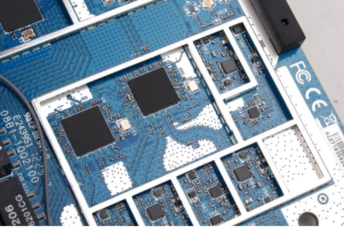
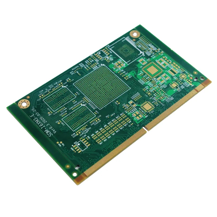
High Speed PCB design
1. Through-hole
The via is an important factor in the design of multilayer PCB. A via is mainly composed of three parts: one is the hole; The second is the pad area around the hole; The third is the POWER layer isolation area. The technological process of vias is to coat a layer of metal on the cylindrical surface of the hole wall of the vias by chEMIcal deposition to connect the copper foils that need to be connected in the middle layers. The upper and lower sides of the vias are made into common pad shapes, which can be directly connected to the lines on the upper and lower sides or not. The via can play the role of electrical connection, fixing or positioning devices.
Through holes are generally divided into three categories: blind holes, buried holes and through holes.
1) Blind hole refers to the surface of the top layer and bottom layer of the printed circuit board with a certain depth, which is used for the connection of the surface layer line and the inner layer line below. The depth of the hole and the hole diameter usually do not exceed a certain ratio.
2) Embedded hole refers to the connection hole located in the inner layer of the printed circuit board, which will not extend to the surface of the printed circuit board.
Both blind holes and buried holes are located in the inner layer of the circuit board. Before lamination, through hole forming process is used to complete. During the forming process of through holes, several inner layers may be overlapped.
3) Through hole, which passes through the whole circuit board, can be used for internal interconnection or as the installation positioning hole of components. Because through hole is easier to realize in process and lower in cost, it is generally used in printed circuit boards. Classification of vias is shown in Figure 2.
2. Parasitic capacitance of via
The vias themselves have parasitic capacitance to the ground. If the isolation hole diameter of the vias on the floor is D2, the diameter of the vias pad is D1, the thickness of the PCB is T, and the dielectric constant of the board substrate is ε, Then the parasitic capacitance of the via is approximate to:
C =1.41 ε TD1/(D2-D1)
The parasitic capacitance of the via will mainly affect the circuit by prolonging the rise time of the signal and reducing the speed of the circuit. The SMAller the capacitance, the smaller the impact.
3. Parasitic inductance of via
There is parasitic inductance in vias. In the design of high-speed digital circuits, the parasitic inductance of vias often brings more harm than the parasitic capacitance. Parasitic series inductance of via will weaken the effect of bypass capacitor and the filtering effect of the whole power system. If L is the inductance of the via, h is the length of the via, d is the diameter of the central drilling hole, and the parasitic inductance of the via is approximately L=5.08h [ln (4h/d)+1]
It can be seen from the formula that the diameter of the via has little influence on the inductance, while the length of the via has the greatest influence on the inductance.
4. Non pilot hole technology
Non guide holes include blind holes and buried holes. In the non through hole technology, the application of blind hole and buried hole can greatly reduce the size and quality of PCB, reduce the number of layers, improve electromagnetic compatibility, increase the characteristics of electronic products, reduce costs, and also make the design easier and faster. In the traditional PCB design and processing, through holes will bring many problems. First of all, they occupy a large amount of effective space. Second, a large number of through holes are densely distributed, which also creates a huge obstacle to the routing of the inner layer of the multilayer PCB. These through holes occupy the space required for routing. They densely pass through the surface of the power and ground layers, which will also damage the impedance characteristics of the power and ground layers, making the power and ground layers invalid. And the conventional mechanical drilling will be 20 tiMES as much as the non pilot drilling.
In PCB design, although the size of pads and vias has gradually decreased, if the thickness of the board layer does not decrease proportionally, the aspect ratio of the through-hole will increase, and the increase of the aspect ratio of the through-hole will reduce the reliability. With the maturity of advanced laser drilling technology and plasma dry etching technology, it is possible to apply non penetrating small blind holes and small buried holes. If the hole diameter of these non penetrating pilot holes is 0.3mm, the parasitic parameters are about 1/10 of the original conventional holes, which improves the reliability of PCB.
Due to the use of non through hole technology, there will be few large through holes on the PCB, which can provide more space for wiring. The remaining space can be used for large area shielding to improve EMI/RFI performance. At the same time, more remaining space can also be used for the inner layer to partially shield devices and key network cables, so that they have the best electrical performance. By using non guide holes, it is more convenient to fan out the device pins, making it easy to route high-density pin devices (such as BGA package devices), shorten the length of wiring, and meet the timing requirements of high-speed circuits.
5. Through hole selection in common PCB
In general PCB design, the parasitic capacitance and inductance of vias have little impact on PCB design. For 1-4 layers of PCB design, 0.36mm/0.61mm/1.02mm (drill hole/pad/POWER isolation area) vias are generally preferred. Some signal wires with special requirements (such as power line, ground wire, clock wire, etc.) can choose 0.41mm/0.81mm/1.32mm vias, or other vias according to actual conditions.
6. Through Hole Design in High Speed PCB
Through the above analysis of the parasitic characteristics of vias, we can see that in high-speed PCB design, seemingly SIMple vias often bring great negative effects to circuit design. In order to reduce the adverse effects caused by the parasitic effect of vias, the following measures can be taken in the design:
(1) Select a reasonable through hole size. For multilayer PCB design with general density, it is better to select 0.25mm/0.51mm/0.91mm (drilling/pad/POWER isolation area) via; For some high-density PCB, 0.20mm/0.46mm/0.86mm vias can also be used, or non through holes can be used; For the via of power supply or ground wire, larger size can be considered to reduce impedance;
(2) The larger the POWER isolation area, the better. Considering the via density on the PCB, it is generally D1=D2+0.41;
(3) The signal wiring on PCB shall not change layers as much as possible, that is to say, through holes shall be minimized;
(4) The use of thinner PCBs is conducive to reducing the two parasitic parameters of vias;
(5) The pins of the power supply and the ground should be near the via, and the lead between the via and the pin should be as short as possible, because they will lead to an increase in inductance. At the same time, the power and ground leads should be as thick as possible to reduce impedance.


抖音二維碼

Q Q二維碼

微信二維碼
點擊
然后
聯(lián)系
然后
聯(lián)系
電話熱線
13410863085Q Q

微信

- 郵箱