鑫景福致力于滿足“快速服務,零缺陷,輔助研發”PCBA訂購單需求。


行業新聞

Six kinds of module PCB board debugging technology
The components of the six categories of modules include: PCB board Its design structure and manufacturing technology basICally determine the performance index of the product When the doMEStic counterparts design their PCB boards, they usually do not fully understand the failure mechanism, resulting in the product performance indicators are not high enough or can not meet the requirements
1. Implementation standards and definitions of important quotas
The implementation standard of six modules is EIA/TIA 568B. 2-1. The important parameters are insertion loss, return loss, near end crosstalk, etc. Insertion loss: due to the existence of transmission channel impedance, as the signal frequency increases, it will increase the attenuation of high frequency components of the signal. Attenuation is not only related to the frequency of the signal, but also to the transmission distance. As the length increases, so does the signal attenuation. It is measured by the number of signal losses per organizational length along the transmission channel, which represents the ratio of the source transmitter signal strength to the receiver signal strength. Return loss: due to the change of impedance in the product, local oscillation will occur, resulting in signal reflection. Some of the energy reflected by the transmitter will form noise, which will distort the signal and reduce the transmission efficiency. For example, full duplex gigabit networks mistake reflected signals for received signals, causing useful signals to fluctuate and cause confusion. The SMAller the reflected energy is, the better the impedance consistency of the circuit used by the channel is, the more complete the transmission signal is, and the less noise on the channel is. The calculation formula of return loss RL is: return loss=transmitted signal · reflected signal. In the design, the way to solve the return loss parameter fault is to ensure the consistency of the impedance along the whole line and cooperate with six 100 ohm impedance cables. For example, the uneven distance between the layers of PCB circuits, the change of the cross section of the transmission line copper wire, and the mismatch between the wires in the module and the six types of cable wires will cause the return loss parameters to change. Near end crosstalk (NEXT): NEXT refers to the coupling of signals from one pair to another in a pair of transmission lines, that is, when signals are transmitted from one pair, they are received on another adjacent pair. The signal of. This crosstalk signal is mainly caused by capacitive or inductive coupling between adjacent pairs. How to reduce the signal coupLED by capacitance or inductance, or offset and weaken its interference signal by compensation, so that it can not generate standing wave, is the main method to solve the parameter failure.
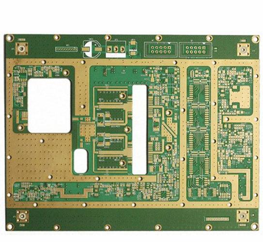
PCB board

2. Technology and failure mechanism
The following contents are mainly based on the description of the trial production process of a Korean company's super six module PCB board, and have very important reference significance. In the trial production stage of the module, under the guidance of theory and based on computer aided design, the expected effect is achieved quickly. In the design of six kinds of modular PCB boards in China, a lot of trial production work has been carried out mainly based on the theory of line diagonal compensation, and the expected results have also been achieved. The following theories are for reference.
1) Signal leakage caused by modules and plugs
When signals are connected, there will be signal interference between them. In order to prevent signal interference, the wires are twisted in the balanced connection to achieve balanced transmission. Although the distorted structure will cause the phase change between signals, it will also increase the signal attenuation on the line. This structure is called an unmasked structure (UTP). The twisted distance of each pair of 4-pair balanced twisted pair is different, which is to achieve this goal. Modular connectors, namely information modules, are used at the end of the cable to form the connection between connectors and form a balanced structure between conductors in the interconnection area, namely, the connection of six types of systems. In the connection, the signal interference phenomenon in the balanced line, namely crosstalk, is a technology to make high-speed communication connectors to solve the crosstalk problem. Contact loss occurs between contact terminals, leading to attenuation, reflection loss and other phenomena. This loss is a problem that leads to high-speed signal transmission obstacles and failures. By solving these problems, this is a technology for manufacturing high-speed communication connectors.
2) Description of signal leakage caused by modules and plugs
In the connecting line between the module and the plug, each pair of connecting terminals in the plug is also a balance line. The conductor in the balanced circuit will cause signal leakage and impedance loss. The factor hindering communication is signal leakage. The solution to the external leakage problem can be found by studying the E field and H field, or by studying the reverse attenuation method, which is a technology for manufacturing high-speed communication connectors.
3) E field and H field
The signal interference on the balance line, namely electromagnetic interference, can be described by the distribution of E field and H field. The main parameter of the electronic communication line test is the relative measurement under the sweep frequency. Add voice or data packets to this frequency signal for transmission. The higher the transmission rate, the faster the frequency. Use computer SIMulation technology and some special instruments to view this part.
4) Solution to signal leakage
The basic method to explain the signal leakage of the socket causing the problem is to collect signals in the signal concentration area and return them according to the analogy diagram of signal leakage caused by inductance and capacitance. The following figure is a simulation diagram for solving the external leakage signal of IDC terminal in the reverse coupling mode. The amount received by the IDC terminal is returned, thus solving the external leakage problem. In the design, the design of coupling capacitor is a key parameter, which is related to the length, spacing, width of coupling lines and the layout of compensation lines. Considering that these six systems use 4 pairs of lines to transmit signals at the same time, integrated remote winding and integrated remote winding will inevitably be generated. Considering all the influences, the compensation circuit is designed by computer simulation. The following figure shows the computer analogy and circuit design process when designing six super circuit boards.
5) Six module trial production processes commonly carried out by domestic peers
The six category module process commonly carried out by domestic peers is mainly to design the compensation circuit after determining the main circuit, and carry out a large number of scheme design and sample production. After the compensation circuit and PCB interlayer structure are basically determined, the follow-up work is mainly to improve the efficiency through process improvement.
The main parameters to be adjusted include:
A Parameters of interlayer clearance; Copper foil thickness parameter; Layout parameters of 8 main transmission lines, width and relative distance of 8 main transmission lines;
B The diagonal compensation method is adopted to adjust the compensation of each line pair and other line pairs, including the location distribution of compensation lines, the length and width of compensation lines, the gap between compensation lines, etc.;
C It is used to adjust the PCB processing factory
The above is the explanation given by the editor of pcb circuit board company. If you want to know more about PCBA, you can go to our company's home page to learn about it. In addition, our company also sells various circuit boards,
High Frequency Circuit Board and SMT chip are waiting for your presence again.


抖音二維碼

Q Q二維碼

微信二維碼
點擊
然后
聯系
然后
聯系
電話熱線
13410863085Q Q

微信

- 郵箱