鑫景福致力于滿足“快速服務(wù),零缺陷,輔助研發(fā)”PCBA訂購單需求。


行業(yè)新聞
Anti electrostatIC discharge method in PCB design
In designing PCB boards, anti-statIC design PCB boards can be realized through layering, correct layout, and installation During the design process, most design modifications can be limited to adding or removing components through prediction ESD can be well prevented by adjusting PCB Here are some common precautions Use as many multilayer PCB boards as possible Compared with double-sided PCB boards, ground and power planes, and closely arranged signal line ground spacing can reduce common mode impedance and inductive coupling, making it possible to realize double-sided printing on PCB boards 1./10 to 1/Page 100 Try to place each signal layer close to the power layer or ground plane For high-density PCB with components on the top and bottom surfaces, with very short interconnects, and many ground fillers, consider using an inner layer
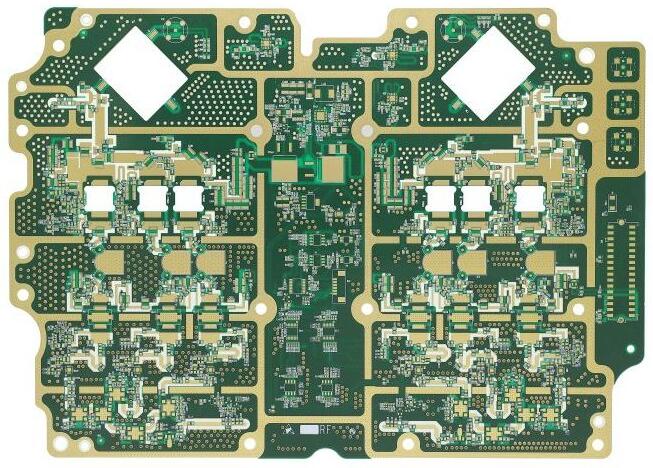
PCB board

For double-sided PCB, tightly interwoven power supply and grounding grid shall be used. The power cord is close to the ground wire, and there are as many connections between the vertical and horizontal conductors or pads as possible. The grid size on one side is less than or equal to 60mm, and if possible, the grid size should be less than 13mm. Ensure that each circuit is as compact as possible. Place all connectors aside as far as possible. If possible, pass the power cable through the center of the card and away from the area directly affected by electrostatic discharge. Place the wide host shell grounding or polygon filler on all PCB layers under the connectors LED out from the host shell (easy to be directly impacted by ESD), and connect them together with vias about 13mm apart. Place the mounting hole on the edge of the card, and pad the top and bottom around the mounting hole with no solder until the main housing is grounded. During PCB assembly, do not apply any solder to the top or bottom pads. Use the screws with included washers to make the PCB board in close contact with the metal main housing/mask or bracket on the ground plane. Set the same "isolation zone" between chassis grounding and circuit grounding of each layer; If possible, maintain a separation distance of 0.64 mm. At the top layer and bottom layer of the card close to the mounting hole, 1.27mm wide wires are used to connect the main housing grounding and circuit grounding every 100mm along the main housing grounding wire. Place pads or mounting holes near these connection points for installation between chassis ground and circuit ground. These ground connections can be cut with a blade to keep them open, or they can be bridged with ferrite beads/high-frequency capacitors.
If the circuit board will not be placed in the metal host shell or mask, please do not apply solder resist on the top and bottom host shell grounding of the circuit board, so that they can be used as the discharge electrode of the ESD arc. Ring grounding shall be set around the circuit with the following pipes:
(1) In addition to the edge connector and chassis grounding, place a ring grounding path around the entire perimeter.
(2) Ensure that the annular width of all layers is greater than 2.5mm.
(3) Ring connection through holes every 13mm.
(4) Connect the ring ground to the common ground of the multilayer circuit.
(5) For double-sided panels installed in metal cabinets or shielding devices, the ring ground should be connected to the circuit common ground. For unshielded double-sided circuits, the ring ground should be connected to the main housing ground. Solder resistance should not be used for ring grounding, so that the ring grounding can be used as the discharge rod of electrostatic discharge. Place at least one position (all layers) on the circular ground. 0.5mm wide gap to avoid large loop. The distance between signal wire and ring grounding shall not be less than 0.5mm.
In the area where electrostatic discharge can directly hit, the grounding wire shall be laid near each signal line. The input/output circuit shall be as close to the corresponding connector as possible. Circuits susceptible to electrostatic discharge should be close to the center of the circuit so that other circuits can provide some masks for them. Generally, a series resistor and magnetic bead are placed at the receiving end. For cable drivers that are easy to be shocked by electrostatic discharge, a series resistor or magnetic bead can also be placed at the driving end. The transient protector is usually placed at the receiving end. Use short and thick wires (less than 5 tiMES the width, less than 3 times the width) to connect to the main housing for grounding. The signal wire and ground wire from the connector shall be directly connected to the transient protector before connecting to the rest of the circuit. The filter capacitor shall be placed at the connector or within 25mm from the receiving circuit.
(1) Use short and thick wires to connect to the main housing ground or the receiving circuit ground (the length is less than 5 times the width and less than 3 times the width).
(2) The signal line and ground wire are first connected to the capacitor, and then to the receiving circuit.
Make sure the signal line is as short as possible. When the length of signal line is greater than 300mm, the ground wire must be laid in parallel. Ensure that the loop area between the signal line and the corresponding loop is as SMAll as possible. For long signal lines, the positions of signal lines and ground wires need to be changed every few centimeters to reduce the loop area. The signal is driven from a central location in the network to a plurality of receiving circuits. To ensure that the loop area between the power supply and the grounding is as small as possible, a high-frequency capacitor is placed near each power pin of the IC chip. Place a high-frequency bypass capacitor within 80mm of each connector. Where possible, fill unused areas with ground, connecting all layers of filled ground every 60mm. Make sure to connect to the ground at two opposite ends of any large ground fill area (approximately larger than 25mm x 6mm). When the length of the opening in the power supply or ground plane exceeds 8mm, use narrow wires to connect both sides of the opening. The reset line interrupt signal line or edge trigger signal line cannot be placed near the PCB edge. Connect the mounting hole to the circuit common or isolate it.
(1) When metal support must be used with metal mask device or chassis, zero ohm resistor shall be used for connection.
(2) Determine the size of the mounting hole to achieve reliable installation of metal or plastic support. Use large mats on the top and bottom layers of the mounting holes. Do not use solder resist on the bottom pad and ensure that the bottom pad is not wave welded. Welding.
The protected signal lines and unprotected signal lines cannot be arranged in parallel. Pay special attention to the routing of reset, interrupt and control signal lines.
(1) High frequency filtering shall be used.
(2) Keep away from input and output circuits.
(3) Keep away from the edge of the circuit board.
This PCB should be inserted into the main housing and not installed in the opening or inner seam Note the wiring under the bead, between the pads, and the signal wires that may contact the beads Some magnetic beads are very conductive and may have unexpected conductive paths If a main housing or main board will contain multiple circuit boards, the electrostatic sensitive PCB board should be placed in the middle
The above is the explanation given by the editor of pcb circuit board company. If you want to know more about PCBA, you can go to our company's home page to learn about it. In addition, our company also sells various circuit boards,
High Frequency Circuit Board and SMT chip are waiting for your presence again.
Wet and PCB board surface treatment
11-04,2022


抖音二維碼

Q Q二維碼

微信二維碼
點(diǎn)擊
然后
聯(lián)系
然后
聯(lián)系
電話熱線
13410863085Q Q

微信

- 郵箱