鑫景福致力于滿足“快速服務,零缺陷,輔助研發”PCBA訂購單需求。


行業新聞
Pcb factory: factors causing poor contact of test probe after welding
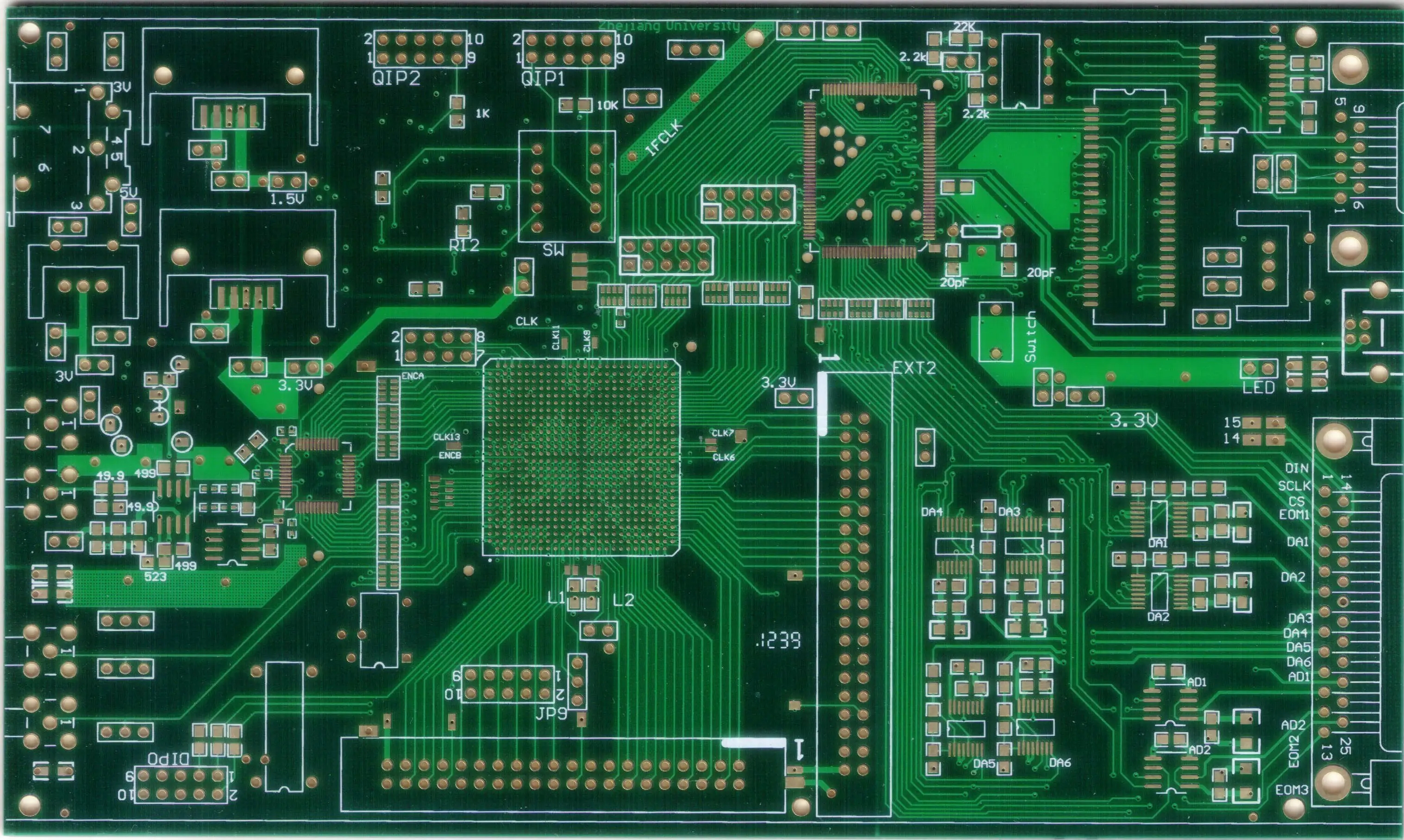
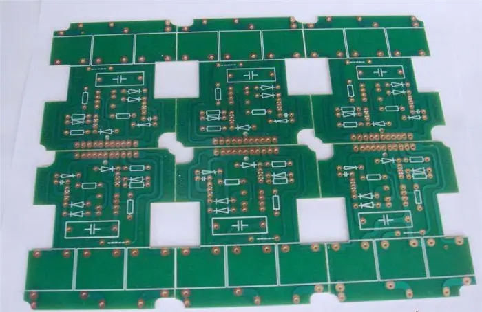
1. Factors that cause poor contact of the test probe after welding During in-line testing of the circuit board, poor contact may occur due to the residue of reflow, whICh is of course due to the insulating residue between the test probe and the test pad or solder joint. Due to the consideration of ozone layer destruction and work health and safety, as well as the attempt to save costs, the wash free process technology has rapidly become the mainstream technology of SMT assembly. The elimination of cleaning procedures can not only avoid the pollution caused by the use of cleaning agents, but also eliminate the steps and processes of cleaning and all necessary costs. In addition, in order to further enhance the advantages of the wash free process
1. Factors causing poor contact of test probe after welding
During in line testing of circuit boards, poor contact may occur due to the residue of reflow, which is of course due to the insulation residue between the test probe and the test pad or solder joint. Due to the consideration of ozone layer destruction and work health and safety, as well as the attempt to save costs, the wash free process technology has rapidly become the mainstream technology of SMT assembly. The elimination of cleaning procedures can not only avoid the pollution caused by the use of cleaning agents, but also eliminate the steps and processes of cleaning and all necessary costs.
In addition, in order to further improve the advantages of the wash free process, wave welding technology has been gradually used instead of back welding. However, the main problem in the industry is not the soldering characteristics of circuit boards or the reliability of products, but the problem of in line testing. As there are flux residues on the circuit board, the probe may not be able to penetrate the residue, or it may soon be attached by the residue and finally cannot generate electrical connection. This situation is more serious especially when the test position is at the end of the pin or the end of the lead pin of the through-hole part. Obviously, flux residue is one of the most important reasons for this problem.
Of course, it is also mentioned that the problem can be overcome by increasing the probe pressure. However, in the face of possible damage to the product welding point and the probe itself, the overall operation cost and the life of the fixture also test the applicability of this approach.
2. Methods to avoid
Through the research on the influence of circuit board tester on the amount of solder paste residue, it is found that the detectability of equipment and the penetrability of probe will decrease with the increase of the amount of residue for the air reflow system. This result is understandable, because the more flux residues left on the welding pad, the less effective the probe can produce.
However, this trend cannot judge the detectability of the pin end and the penetrability of the through-hole. The amount of solder paste residues in these areas is not necessarily the main factor, but other properties control the probe measurability. These properties include: top diffusion, bottom diffusion, hardness and other factors of flux residue.
In terms of top flux diffusion, the better the flux diffusion, the less residue on the pad. It is reasonable to estimate that the detectability of the pad will increase with the increase of diffusion. However, in the actual situation, the phenomenon occurred is contrary to the speculation, and the top flux diffusivity is inversely proportional to the detectability of the pad.
This abnormal situation is caused by another influencing factor. The solder paste with high residue not only affects the diffusion of the flux, but also generates thick residue deposits on the welding pad, which leads to the generation of low detectable values of the welding pad.
In terms of bottom flux diffusion, although there is no direct trend to distinguish it from pad detectability or through-hole penetrability, it does have a clear relationship with the detectability of pin ends. The detectability value of the pin increases with increasing flux diffusion at the bottom, and also increases with decreasing residue.
The theoretical basis of this phenomenon is the dropping mechanism. The solder paste residues will have low solid content and low viscosity when soldering the circuit board. The low viscosity in the through-hole will allow the flux to flow out of the solder paste and spread rapidly around the bottom surface. If the flux is further diffused at the bottom, less flux will accumulate at the pin, so the test probe can easily penetrate.


抖音二維碼

Q Q二維碼

微信二維碼
點擊
然后
聯系
然后
聯系
電話熱線
13410863085Q Q

微信

- 郵箱