鑫景福致力于滿足“快速服務,零缺陷,輔助研發”PCBA訂購單需求。


行業新聞
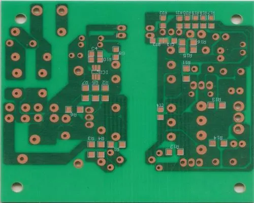
Through hole (VIA) is used to conduct or connect copper foil lines between conductive patterns in different layers of the circuit board, but it is not allowed to insert copper plated holes of component legs or other reinforcement materials. Printed circuit board (PCB) is formed by stacking many copper foil layers. The reason why copper foil layers cannot communICate with each other is that each layer of copper foil is paved with an insulating layer, so they need to rely on via for signal link, so they have the Chinese name of via.
The through hole of the circuit board must pass through the plug hole to meet the customer's needs. In the process of changing the traditional aluminum chip plug hole process, the resistance welding and plug hole of the circuit board surface are completed by using the white MESh, making its production more stable, quality more reliable, and application more perfect. Through hole is helpful for connecting and conducting circuits. With the rapid development of electronic industry, higher requirements are put forward for the fabrication of Printed Circuit Board (PCB) and surface STM technology.
Plug hole technology of through hole arises at the historic moment, and at the same time, the following requirements shall be met:
1. The hole only needs copper, and the resistance welding can be plugged or not plugged;
2. There must be tin and lead in the hole, with a certain thickness requirement (4um), to avoid solder resist ink entering the hole and causing tin beads in the hole;
3. The through hole must be provided with solder blocking ink plug hole, which is light tight, free of tin ring and tin bead, and must be flat.
Blind hole refers to the connection between the outermost circuit in the printed circuit board (PCB) and the adjacent inner layer with plated holes. Since the opposite side cannot be seen, it is calLED blind through. In order to increase the utilization of space between layers of a board circuit, blind holes are used. Blind hole is a through hole to the surface of printed board
The blind hole is located on the top layer and bottom layer of the circuit board, and has a certain depth. It is used to connect the surface layer circuit with the lower inner layer circuit. The depth of the hole generally has a specified ratio (aperture). This fabrication method requires special attention. The drilling depth must be just right. If not, it will cause electroplating difficulties in the hole. Therefore, few factories will adopt this production method. In fact, it is also possible to make the circuit layers that need to be connected in advance drill holes in individual circuit layers, and then glue them together, but it requires more precise positioning and alignment devices.
Buried hole refers to the connection between any circuit layers in a printed circuit board (PCB), but it is not conductive to the outer layer, that is, there is no conductive hole extending to the surface of the PCB.
This PCB manufacturing process cannot be achieved by drilling holes after the circuit board is bonded. Drilling operations must be carried out when individual circuit layers are used. First, the inner layer is partially bonded, then the electroplating process is carried out, and finally, the entire bonding is carried out. Since the operation process is more laborious than the original through hole and blind hole, the price is also the most expensive. This manufacturing process is usually only used for high-density circuit boards to increase the space utilization of other circuit layers.
In the production process of printed circuit board (PCB), drilling is very important. Drilling is SIMply understood as drilling the required through-hole on the CCL, which has the function of providing electrical connection and fixing components. If incorrect operation causes problems in the via process, the components cannot be fixed on the circuit board, which may affect the use of the circuit board, or even make the whole board scrapped, so the drilling process is very important.


抖音二維碼

Q Q二維碼

微信二維碼
點擊
然后
聯系
然后
聯系
電話熱線
13410863085Q Q

微信

- 郵箱