鑫景福致力于滿足“快速服務,零缺陷,輔助研發”PCBA訂購單需求。


行業新聞
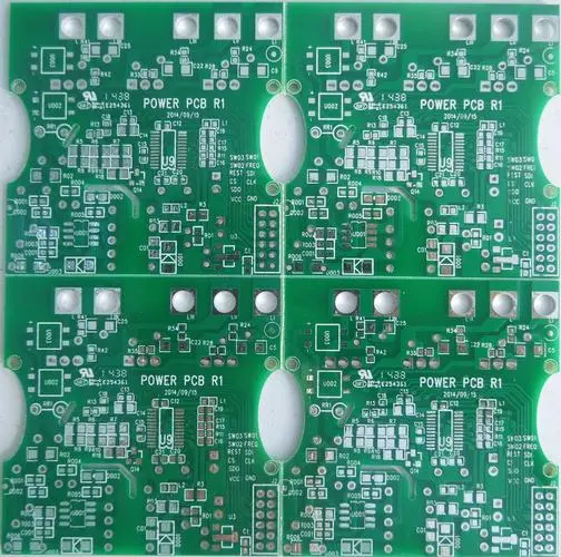
The most commonly used components in the processing of labor and materials are patch materials and plug-in materials, and each has its own advantages. Due to the advantages of miniaturization and precision, SMT processing occupies more and more shares in electronIC processing. chip components are the most used components in SMT OEM. Compared with plug-in components, SMT chip proofing components are SMAll in size and low in cost, but plug-in components also have their own advantages, such as stable performance, good heat dissipation, and better vibration resistance.
Comparison of the advantages of SMT chip proofing parts and plug-in materials.
1. The solder joint defect rate is low.
2. High reliability and strong anti vibration capability.
3. High frequency characteristics, reduce electromagnetic and radio frequency interference.
4. Light weight: the weight of SMT components is only 10% of that of traditional DIP components. After SMT is used, the weight is reduced by 60%~80%.
5. Small size: The volume of PCB components for SMT chip proofing is only about 10% of that of traditional DIP plug-in components. Generally, after SMT chip proofing, the volume of electronic products is reduced by 40%~60%.
6. Low cost: chip processing is easy to realize automation, improve production efficiency, save materials, energy, equipment, manpower, time, etc., and reduce costs by 30%~50%.
Advantages of plug-in components:
2. The failure rate of the plug-in is lower than that of SMT chip proofing, and the inspection is more convenient.
1. When using electronic products with high heat dissipation requirements, the performance of plug-in components will be better than that of SMT processing pasters, because the heat dissipation effect of plug-in materials is very good compared with that of SMT components, and the use of plug-in processing in SMT labor packages will have a better effect on the stability of product performance.
3. In extreme environments, the stability plug-in will perform better in the face of turbulence and vibration. Different components have different advantages, which requires engineers to consider comprehensively in the electronIC design stage so as to select appropriate components to achieve the best effect of SMT processing.
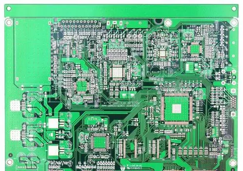
PCB copper coating
Copper coating is to use the idle space on the PCB as the reference plane and then fill it with solid copper. These copper areas are also calLED copper filling. The significance of copper coating is to reduce the ground wire impedance and improve the anti-interference capability; Reduce voltage drop and improve power efficiency; Also, connect with the ground wire to reduce the loop area. If there are many PCBs, such as SGND, AGND, GND, etc., how to cover copper? My approach is to use the most important "ground" as the reference for independent copper coating according to the different surface positions, and to separate the digital and analog copper coating. At the same time, before copper coating, first thicken the corresponding power lines: V5.0V, V3.6V, V3.3V (SD card power supply), etc. In this way, multiple deformation structures with different shapes are formed.
Copper cladding needs to deal with several problems: first, single point connection at different places; second, copper cladding near the crystal oscillator. The crystal oscillator in the circuit is a high-frequency EMIssion source. The method is to coat copper around the crystal oscillator, and then ground the shell of the crystal oscillator separately. Third, there is the problem of isolated islands (dead zones). If you think it is very big, it will not take much to define and add individual vias.
In addition, large area copper coating is better than grid copper coating, which is not easy to generalize. Why? Large area of copper coating, if the wave soldering, the board may be warped, or even bubble. From this point of view, the heat dissipation of the grid is better. Usually, it is a multi-purpose grid with high anti-interference requirements for high-frequency circuits, and a circuit with high current for low-frequency PCB circuits.
PCB copper coating
Add:
In digital circuits, especially those with MCU, the function of copper coating is to reduce the impedance of the whole ground plane for circuits with working frequency above mega. The more specific processing method is generally as follows: each core module (also a digital circuit) will also be coated with copper in different areas when allowed, and then the copper coating will be connected with wires. This is also to reduce the impact of circuits at all levels.
For the mixed circuit of digital circuit and analog circuit, the independent PCB routing of the ground wire and the final summary to the power filter capacitor will not be mentioned, as we all know. However, there is one thing: the distribution of ground wires in analog circuits cannot be SIMply covered with a copper sheet in many cases. Because analog circuits pay much attention to the interaction between the front and rear stages, and analog grounding also requires single point grounding, so whether the analog ground can be covered with a copper sheet must be handled according to the actual situation.


抖音二維碼

Q Q二維碼

微信二維碼
點擊
然后
聯系
然后
聯系
電話熱線
13410863085Q Q

微信

- 郵箱