鑫景福致力于滿足“快速服務,零缺陷,輔助研發(fā)”PCBA訂購單需求。


行業(yè)新聞
In fact, the 8-layer pcb proofing process is SIMilar to that of ordinary circuit boards, but there is more pressing process than ordinary circuit boards. Today, I will show you the specifIC process of 8-layer PCB proofing?
Brief description of the difference between ordinary double-sided pcb board and multilayer PCB board:
The dual panel is a medium layer in the middle, and both sides are cabling layers. Multilayer board is a multi-layer wiring layer. Between each two layers is a dielectric layer, which can be made very thin. The multilayer circuit board has at least three conductive layers, two of which are on the outer surface, and the remaining layer is synthesized in the insulating board. The electrical connection between them is usually realized through the plated through-hole on the cross section of the circuit board.
The production process of 8-layer PCB proofing is the same as that of PCB multilayer board. Let's see what processes are available.
1、 8-layer production - purpose of blackening and browning
① Remove oil stain, impurities and other pollutants on the surface;
② Increasing the specific surface of the copper foil, thereby increasing the contact area with the resin, is conducive to the full diffusion of the resin and the formation of greater adhesion;
③ Make the non-polar copper surface become the surface with polar CuO and Cu2O, and increase the polar bond bonding between copper foil and resin;
④ The oxidized surface is not affected by moisture at high temperature, reducing the probability of copper foil and resin delamination.
⑤ The boards made of the inner circuit must be blackened or browned before laminating. It is used to oxidize the circuit copper surface of the inner plate. Generally, the Cu2O generated is red and the CuO is black, so the Cu2O in the oxide layer mainly refers to browning and the CuO mainly refers to blackening.
1. Lamination is the process of bonding each layer of lines into a whole with the help of B-stage prepreg. This kind of bonding is realized by mutual diffusion and penetration of macromolecules on the interface, and then interweave. The process of bonding each layer of wire into a whole with a sEMI curing sheet. This kind of bonding is realized by mutual diffusion and penetration of macromolecules on the interface, and then interweave.
2. Purpose: Press the discrete multilayer board and the adhesive sheet together to form the multilayer board with the required number of layers and thickness.
① In typesetting, copper foil, bonding sheet (semi curing sheet), inner plate, stainless steel, isolation plate, kraft paper, outer steel plate and other materials are overlapped according to process requirements. If the boards with more than six layers need to be pre typeset. Laminate copper foil, bonding sheet (semi curing sheet), inner plate, stainless steel, isolation plate, kraft paper, outer steel plate and other materials according to process requirements. If the boards with more than six layers need to be pre typeset.
② The laminated circuit board is sent to the vacuum hot press. The heat energy provided by the machine is used to melt the resin in the resin sheet to bond the substrate and fill the gap.
③ Lamination For designers, the first thing to consider in lamination is symmetry. Because the board will be affected by pressure and temperature during the lamination process, there will be stress in the board after the lamination is completed. Therefore, if the two sides of the laminated board are uneven, the stress on both sides will be different, causing the board to bend to one side, which greatly affects the performance of PCB. Keyou Circuit specializes in the production of high-precision multilayer circuit boards. Its products are widely used in such high-tech fields as LCD liquid crystal modules, communication equipment, instruments, industrial power supplies, digital, medical electronics, industrial control equipment, LED modules/modules, power and energy, transportation, science and education research and development, automobiles, aerOSPace and aviation. In addition, even in the same plane, if the distribution of cloth copper is uneven, the resin flow speed at each point will be different, so that the thickness of the place with less cloth copper will be thinner, and the thickness of the place with more cloth copper will be thicker. In order to avoid these problems, the factors such as the uniformity of copper cloth, the symmetry of layers, the design and layout of blind buried holes must be carefully considered in the design.
PCB proofing
2、 8-layer pcb proofing production -- removing dirt and copper deposition
Purpose: To metallize the through hole.
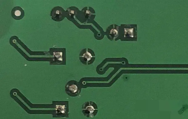
① The substrate of the circuit board is composed of copper foil, glass fiber and epoxy resin. During the fabrication process, the hole wall section after drilling the base material is composed of the above three parts of materials.
② Hole metallization is to solve the problem of covering the section with a layer of uniform, impact resistant metal copper. Hole metallization is to solve the problem of covering the section with a layer of uniform, impact resistant metal copper.
③ The process is divided into three parts: first, the process of drilling dirt, second, the process of chemical copper deposition, and third, the process of thickening copper (full plate copper electroplating).
3、 8-layer pcb proofing - copper sinking and thickening
Hole metallization involves a concept of capability, thickness diameter ratio. The thickness diameter ratio is the ratio of plate thickness to hole diameter., Thickness diameter ratio. The thickness diameter ratio refers to the ratio of plate thickness to hole diameter. When the plate is getting thicker and the hole diameter is decreasing, it is more and more difficult for the chemical yao water to enter the depth of the hole. Although the electroplating equipment uses vibration, pressurization and other methods to let the yao water enter the center of the hole, the thin central coating caused by the concentration difference is still unavoidable. At this time, there will be a micro open circuit in the drilling layer. When the voltage increases and the board is impacted under various adverse conditions, the defects will be completely exposed, causing the circuit of the board to open and unable to complete the specified work.
Therefore, designers need to know the PCB process capability of the board manufacturer in time, otherwise the designed PCB will be difficult to realize in production. It should be noted that the thickness diameter ratio must be considered not only in the through hole design, but also in the blind buried hole design.
4、 8-layer pcb proofing - outer layer dry film and pattern electroplating
The principle of the outer layer pattern transfer is similar to that of the inner layer pattern transfer. Both of them use photosensitive dry film and photographic methods to print the line pattern onto the board. The difference between the outer dry film and the inner dry film is:
① If the reduction method is adopted, the outer dry film is the same as the inner dry film, and the negative film is used as the plate. The cured dry film on the board is PCB circuit. Remove the uncured film, and withdraw the film after acid etching. The circuit pattern remains on the board because of the film protection.


抖音二維碼

Q Q二維碼

微信二維碼
點擊
然后
聯(lián)系
然后
聯(lián)系
電話熱線
13410863085Q Q

微信

- 郵箱