鑫景福致力于滿足“快速服務,零缺陷,輔助研發”PCBA訂購單需求。


行業新聞
Let's understand what is via on PCB
Through hole is one of the important components of multilayer PCB, and the drilling cost usually accounts for 30% - 4.0% of the drilling cost In short, each hole on a PCB can be calLED a through-hole
1. From a functional perspective, vias can be divided into two categories:
1) It is used as the power connection between layers;
2.) Used for fixing or positioning equipment.
In terms of process, these vias are generally divided into three categories, namely blind vias, embedded vias and through vias.
The blind hole is located on the top and bottom surfaces of the printed circuit board. It has a certain depth and is used to connect the surface circuit and the bottom internal circuit. The depth of the hole usually does not exceed a certain ratio (diameter).
Embedded via refers to the connection hole located in the inner layer of the printed circuit board, whICh does not extend to the surface of the circuit board. The above two types of holes are located in the inner layer of the circuit board and are completed by the through hole forming process before lamination. During the formation of through-hole, several inner layers may overlap.
The third type is called through hole, which penetrates the whole circuit board and can be used for internal interconnection or as the installation location hole of components. Because the through-hole is easier to realize in the process of processing and the cost is lower, most printed circuit boards use it to replace the other two kinds of through-hole. Unless otherwise specified, through holes mentioned below are considered as through holes. From the design point of view, the through-hole is mainly composed of two parts, one is the middle drill hole, and the other is the pad area around the drill hole, as shown in the following figure. The size of these two parts determines the size of the through-hole. Obviously, in the design of high-speed and high-density PCB boards, designers always hope that the SMAller the through-hole is, the better, so as to leave more wiring space on the board. In addition, the smaller the through-hole, the smaller its parasitic capacitance, and the more suitable for high-speed circuits. However, the reduction of the hole size also brings new costs, and the size of the through hole cannot be infinitely reduced. It is limited by drilling and electroplating technology: the smaller the hole, the more drilling, the longer the time required, and the easier it is to deviate from the center; When the depth of the hole is more than 6 tiMES of the drilling diameter, uniform copper plating on the hole wall cannot be guaranteed. For example, the thickness (through hole depth) of an ordinary 6-layer PCB is about 50Mil, and the hole diameter provided by the PCB manufacturer can only reach 8Mil.
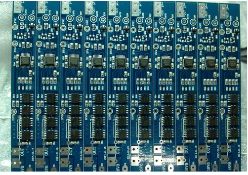
PCB board

2. Parasitic capacitance of via The via itself has parasitic capacitance to ground. If it is known that the diameter of the isolation hole of the via on the ground plane is D2, the diameter of the via pad is D1, and the thickness of the PCB board is T, then the dielectric constant of the board substrate is Q, then the parasitic capacitance of the via is SIMilar to C=1.41 Q TD1/(D2-D1). The main effect of via parasitic capacitance on the circuit is to prolong the rise time of the signal and reduce the speed of the circuit.
For example, for a PCB with a thickness of 50Mil, if a through-hole with an inner diameter of 10Mil and a pad diameter of 20Mil is used, and the distance between the pad and the grounding copper area is 32Mil, the through-hole can be approximately calculated by the above formula. Parasitic capacitance roughness:
C=1.41x4.4x0.050x0.020/(0.032-0.020)=0.517pF,
The rise time change caused by this part of capacitance is:
T10-90=2.2C(Z0/2)=2.2x0.517x(55/2)=31.28ps。
From these values, it can be seen that although the influence of rise and delay caused by parasitic capacitance of a single via is not obvious, if vias are used for switching between layers for many times in the trajectory, the designer should still carefully consider.
3. Parasitic inductance of vias is similar to that of vias. Parasitic capacitance and inductance of vias exist together. In the design of high-speed digital circuits, the harm of via parasitic inductance is often greater than that of parasitic capacitance. Its parasitic series inductance will weaken the contribution of bypass capacitors and reduce the filtering effect of the entire power system. We can easily calculate the approximate parasitic inductance of vias with the following formula: L=5.08h [ln (4h/d)+1]
Where L is the inductance of the through-hole, h is the length of the through-hole, and d is the diameter of the central drilling hole. It can be seen from the formula that the diameter of the through-hole has little effect on the inductance, while the length of the through-hole has an effect on the inductance. Using the above example, the inductance of the through-hole can be calculated as: L=5.08x0.050 [ln (4x0.050/0.010)+1]=1.015nH. If the rise time of the signal is 1ns, its equivalent impedance is XL=L/T10-90=3.19 ?). When high frequency current passes through, this impedance can no longer be ignored. It should be noted that when connecting the power layer and the ground plane, the bypass capacitor needs to pass through two vias to multiply the parasitic inductance of the vias.
4. Through the above analysis of the parasitic characteristics of vias, we can see that in the design of high-Speed PCB boards, seEMIngly simple vias often bring a lot to circuit design. Negative impact. In order to reduce the adverse effects caused by via parasitic effects, you can try as much as possible in the design:
1) Considering the cost and signal quality, the through-hole with reasonable size is selected. For example, for 6-10 layer memory module PCB design, it is better to use 10/20Mil (drilling/pad) through-hole. For some high-density Small circuit boards, 8/18 mils can also be used. Through hole. Under current technical conditions, it is difficult to use smaller vias. For power or grounding vias, consider using a larger size to reduce impedance.
2) From the two formulas discussed above, it can be concluded that the use of thinner PCB is beneficial to reduce the two parasitic parameters of vias.
3) Try not to change the layer of the signal trace on the PCB, that is, try not to use unnecessary vias.
4) The pins for power and ground should be as close to the drill hole as possible. The leads between the through-hole and the pin should be as short as possible because they add inductance. At the same time, the power and grounding leads should be as thick as possible to reduce impedance.
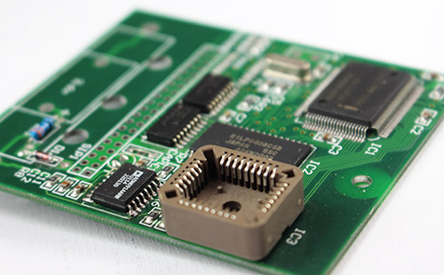
5) Place some grounded vias near the vias where the signal changes layers to provide a short return path for the signal A large number of redundant grounding vias can even be placed on the PCB Of course, flexibility is also required in the design In the case that each layer has pads, we discussed the via model previously. Sometimes, we can reduce or even remove pads from some layers Especially in the case of very high via density, it may lead to the formation of circuit breakers on the copper layer To solve this problem, in addition to moving the position of vias, we can also consider placing vias on the copper layer The pad size is reduced to PCB board


抖音二維碼

Q Q二維碼

微信二維碼
點擊
然后
聯系
然后
聯系
電話熱線
13410863085Q Q

微信

- 郵箱