鑫景福致力于滿足“快速服務,零缺陷,輔助研發”PCBA訂購單需求。


行業新聞

Finite Element Thermal Reliability Analysis of PCB Key Components
With the continuous miniaturization of electronIC equipment, hot PCB design becoMES more and more important SMAll size and compact layout lead to higher temperature rise of components, which greatly reduces the reliability of the system Therefore, starting from the heat transfer principle, this paper uses ANSYS finite element software to analyze the temperature field distribution of the key components of the Printed Circuit Board (PCB) during operation, and determine the high temperature and low temperature areas of the PCB. The temperature fields of different PCB layouts are calculated by an example, and a more reasonable layout method is obtained by comparison Optimize the layout, reduce the engine temperature PCB, and improve the reliability of the system
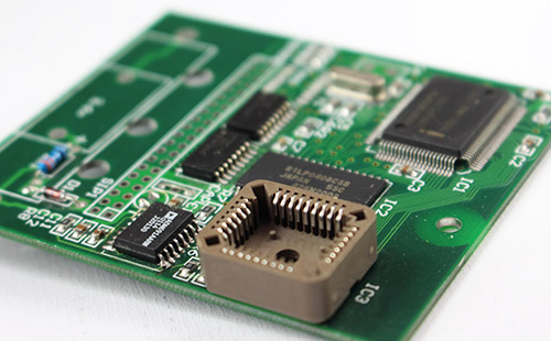
PCB board

1 Introduction
The continuous miniaturization of electronic equipment makes the PCB layout more and more compact. However, unreasonable PCB layout seriously affects the heat transfer path of electronIC components on the board, which leads to the reliability failure of electronic components due to temperature rise, that is, the system reliability is greatly reduced. This also makes the problem of PCB temperature rise rise to a certain height. It is reported that 55% of electronic equipment failure factors are caused by temperature exceeding the specified value. For electronic equipment, even if the temperature is reduced by 1 ° C, the failure rate of the equipment will be greatly reduced. For example, statistics show that the failure rate of civil aviation electronic equipment will be reduced by 4% every 1 ℃. It can be seen that temperature rise control (thermal design) is a very important issue. The heat on the printed circuit board mainly comes from power consumption components, such as transformers, high-power transistors and high-power resistors. Their power consumption is mainly dissipated to the surrounding medium in the form of heat conduction, convection and radiation, and only a small part is dissipated in the form of electromagnetic waves. In order to improve the stability and reliability of electronic components on the PCB, it is necessary to clearly understand the power consumption of key components on the PCB and the temperature field distribution on the board, so as to achieve a reasonable layout. In heat analogy, the finite element or finite difference method is usually used to solve the heat transfer and fluid flow equations. This paper uses finite element analysis. The finite element method is more accurate in solving complex geometry, allowing you to refine the mesh in certain areas (such as the parts of plates or systems that are more interesting than other areas). You can refine the mesh in these areas, while refining the mesh in other areas. A little sparse. However, mesh refinement cannot directly jump from one density to another, and can only be done gradually.
2. Basic Principles of Heat Transfer and ANSYS Finite Element Thermal Analogy Process
ANSYS finite element thermal analogy process
In this paper, ANSYS software is used to build geometric models, and bottom-up and top-down methods are used to build solid models. In the process of building the solid model, due to the complex structure of the electronic components, in order to facilitate the mesh generation and the accuracy of the results, the solid model can be SIMplified, and 87 SOLID 10 node elements suitable for irregular shape element generation are selected.
3. Finite element solution of temperature field
3.1 Example analysis of two-dimensional temperature field
Layout 1: chip1, Chip2 side by side, Chip3 next to Chip1. The temperature is 101.5 ° C and 92.7 ° C.
Layout 2: The chip 1 and chip 2 are side by side on one side of the PCB, and the chip 3 is on the other side of the PCB. The temperature is 90 ° C and the temperature is 70.7 ° C.
3.2 Comparative analysis
1) Comparing the analysis results of the two final analog temperature fields, it can be clearly found that the temperature and temperature of Layout 2 have been greatly reduced (about 10 ?? twenty ??), This is very impressive for the thermal reliability of electronics. For example, statistics show that the failure rate of civil aviation electronic equipment will be reduced by 4% every 1 ℃. It can be seen that temperature rise control (thermal design) is a very important issue. So as to improve the reliability of the equipment.
2) The two temperature field distribution maps both reflect the same problem: when the components are densely distributed, the temperature field distribution is irregular, and the high temperature and low temperature areas cannot be determined. In this case, when arranging PCB boards, full attention should be paid to the dense area of power consumption components, in which components with low thermal sensitivity should not be placed or placed as far as possible.
3) The convection heat transfer coefficient in the finite element analysis is different for different component values. If only the point measurement results are used for calculation, the value of h will be very small, so some corrections must be made. The h value with large power consumption is slightly larger, then compare the calculation result with the measurement result, and continuously adjust the h value until it is basically consistent.
4) In different temperature field distributions, although the colors displayed are the same, the temperature values represented by the same color are different. They are used to instruct the trend from high temperature area to low temperature area.
5) The boundary conditions are also very important. The boundary conditions given in the modeling process must be correct.
Example analysis of 3.33 dimensional temperature field
There are 3 chips on the PCB, and the layout and all parameters are the same as 2.
4. Conclusion and analysis
1) On the surface, the 3D temperature field analogy is not as ideal as the 2D temperature field analogy, but this is not the case. The temperature displayed in the 3D analogy is the mold position of the component, where the temperature is actually higher than the surface temperature of the component. Recall that the simulation result of Layout 2 is reasonable.
2) 3D models are more complex. For the accuracy of simulation results, the wafer data can be considered as three layers of different data to simplify the model.
3) The establishment of 3D model and the processing of results cost a lot of energy and time. The data and structure requirements are more detaiLED and specific than the 2D model Although 3D analogy can obtain more information, 2D can also quickly obtain approximate temperature field distribution Therefore, in practical application, these two methods can be based on the actual situation of PCB
?About PCBA welding type and method
11-07,2022


抖音二維碼

Q Q二維碼

微信二維碼
點擊
然后
聯系
然后
聯系
電話熱線
13410863085Q Q

微信

- 郵箱