鑫景福致力于滿足“快速服務,零缺陷,輔助研發”PCBA訂購單需求。


行業新聞

In this step, the PCB surface is drawn in the PCB design environment according to the determined PCB size and various mechanICal positioning, and the required connectors, keys/switches, screw holes, assembly holes, etc. are placed according to the positioning requirements. And fully consider and determine the wiring area and non wiring area (such as how large the area around the screw hole belongs to the non wiring area).
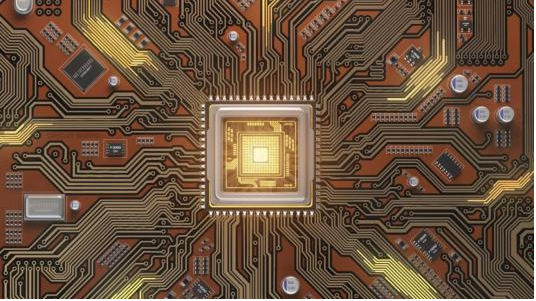
PCB layout
① According to the reasonable division of electrical performance, it is generally divided into: digital circuit area (i.e., fear of interference and generate interference), analog circuit area (fear of interference), power drive area (interference source);
e as possible, and all components shall be adjusted to ensure the most concise connection; At the same time, adjust the relative position between the function blocks to make the connection between the function blocks the most concise;
③ For components with high quality, the installation position and strength shall be considered; The heating element shall be placed separately from the temperature sensing element, and thermal convection measures shall be considered when necessary;
④ The I/O driver shall be close to the edge of the printed board and the outlet connector as far as possible;
⑤ The clock generator (such as crystal oscillator or clock oscillator) shall be as close as possible to the device using the clock;
⑥ A decoupling capacitor shall be added between the power input pin of each integrated circuit and the ground (generally, a monolithic capacitor with good high-frequency performance is used); When the circuit board space is dense, a tantalum capacitor can also be added around several integrated circuits;
⑦ A discharge diode (1N4148) shall be added at the relay coil;
⑧ The layout should be balanced, dense and orderly, not top heavy or heavy.
Special attention shall be paid to the actual size (area and height) of components and the relative position between components during placement to ensure the electrical performance of the circuit board and the feasibility and convenience of production and installation. At the same time, the placement of components shall be properly modified to make them neat and beautiful on the prEMIse that the above principles can be reflected. The same components shall be placed orderly and in the same direction, It should not be placed in an "orderly manner".
This step is related to the overall image of the board and the difficulty of wiring in the next step, so we should make great efforts to consider it. In the layout, preliminary wiring can be made for uncertain places, and full consideration can be given.
Wiring is the most important process in PCB design. This will directly affect the performance of PCB. In the process of PCB design, there are generally three levels of wiring: first, routing, which is the most basic requirement for PCB design. If the lines are not connected and there are flying lines everywhere, it will be an unqualified board. It can be said that we haven't started yet.
PCB design
The second is the satisfaction of electrical performance. This is the standard to measure whether a printed circuit board is qualified. This is to carefully adjust the wiring after wiring to achieve the best electrical performance.
Next is beauty. If your wiring is connected, there is no place that affects the performance of electrical appliances. But at a glance, it is chaotic, colorful and colorful. Even if your electrical performance is good, it is still a piece of garbage in the eyes of others. This brings great inconvenience to testing and maintenance. The wiring shall be neat and uniform, and shall not be crisscross and disorganized. All these should be achieved under the premise of ensuring the electrical performance and meeting other individual requirements, otherwise, it will be a waste of time.
The wiring shall be carried out according to the following principles:
① In general, the power line and ground wire shall be wired first to ensure the electrical performance of the circuit board. Within the allowable range, the width of power supply and ground wire shall be widened as much as possible. It is better that the ground wire is wider than the power wire. Their relationship is: ground wire>power wire>signal wire. Generally, the width of signal wire is 0.2~0.3mm, the thinnest width can reach 0.05~0.07mm, and the power wire is generally 1.2~2.5mm. The PCB of digital circuit can be used to form a loop with a wide ground wire, that is, to form a ground grid for use (the ground of analog circuit cannot be used in this way)
② PCB wiring process requirements:
In general, the signal line width is 0.3mm (12mil), and the power line width is 0.77mm (30mil) or 1.27mm (50mil); The distance between lines and between lines and pads shall be greater than or equal to 0.33mm (13mil). In practical application, if conditions permit, the distance shall be increased;
When the wiring density is high, it can be considered (but not recommended) to use two lines between IC pins, the width of the line is 0.254mm (10mil), and the line spacing is not less than 0.254mm (10mil). Under special circumstances, when the device pins are dense and the width is narrow, the line width and line spacing can be appropriately reduced.
The basic requirements for PAD and VIA are: the diameter of PAD is greater than that of hole by 0.6 mm; For example, universal pin resistors, capacitors and integrated circuits are 1.6mm/0.8mm (63mil/32mil) in panel/hole size, 1.8mm/1.0mm (71mil/39mil) in socket, pin and diode 1N4007. In practical application, it shall be determined according to the size of the actual component. If possible, the pad size can be appropriately increased; The component installation hole diameter designed on the PCB shall be 0.2~0.4mm larger than the actual size of the component pin.
③ Via (VIA): 1.27mm/0.7mm (50mil/28mil) generally; When the wiring density is high, the via size can be appropriately reduced, but should not be too SMAll, and 1.0mm/0.6mm (40mil/24mil) can be considered.
④ Spacing requirements for pads, wires and vias
PAD and VIA :≥ 0.3mm(12mil)
PAD and PAD :≥ 0.3mm(12mil)
PAD and TRACK :≥ 0.3mm(12mil)
TRACK and TRACK :≥ 0.3mm(12mil)
When the density is high:
PAD and VIA :≥ 0.254mm(10mil)
PAD and PAD :≥ 0.254mm(10mil)
PAD and TRACK :≥ 0.254mm(10mil)
TRACK and TRACK :≥ 0.254mm(10mil)
Routing optimization and silk screen
"There is no best, only better"! No matter how much you try to design, after painting, you will find that there are many places that can be modified. The general design experience is that the time for optimal routing is twice as long as the time for initial routing.
I don't think there is anything that needs to be modified. After that, I can lay copper (Place ->polygon plane). Copper is generally laid with ground wire (pay attention to the separation of analog ground and digital ground), and power supply may also be required for multi-layer boards. For silk screen, it should be noted that it cannot be blocked by devices or removed by vias and pads. At the same time, when designing, face up to the component surface, and the characters at the bottom layer should be mirrored to avoid confusing the layers.
Network and DRC check and structure check
First, on the premise of confirming that the circuit schematIC design is correct, NETCHECK the generated PCB network file and the schematic network file for the physical connection relationship, and correct the design in time according to the output file results to ensure the correctness of the wiring connection relationship; After the network check is passed correctly, DRC check shall be carried out on the PCB design, and the design shall be corrected in time according to the output file results to ensure the electrical performance of PCB wiring. Finally, the mechanical installation structure of PCB needs to be further checked and confirmed.
Plate making
① Before that, it is better to have an audit process.
PCB design is a mental work. The Board Designed by the person who is thoughtful and experienced is good. Therefore, we should be extremely careful in design, fully consider all factors (for example, many people do not consider the convenience of maintenance and inspection), and strive for perfection, so that we can design a good board.
② Wires with strict requirements (such as high-frequency lines) shall be wired in advance. The side lines of input and output terminals shall not be adjacent and parallel to each other to avoid reflection interference. If necessary, ground wires shall be added for isolation, and the wiring of two adjacent layers shall be perpendicular to each other, which may cause parasitic coupling.
③ The oscillator shell shall be grounded, and the clock line shall be as short as possible, and shall not be LED everywhere. The area of the ground under the clock oscillation circuit and special high-speed logic circuit should be added, and other signal lines should not be used to make the surrounding electric field approach zero;
④ 45 ° broken lines shall be used as far as possible, and 90 ° broken lines shall not be used to reduce the radiation of high-frequency signals; (Double arc shall be used for lines with high requirements);
⑤ No signal line shall form a loop. If it is unavoidable, the loop shall be as small as possible; The vias of signal lines shall be as few as possible;
⑥ The key lines shall be as short and thick as possible, and protective areas shall be added on both sides;
⑦ When transmitting sensitive signals and noise field band signals through flat cables, they should be led out in the way of "ground wire signal ground wire";
⑧ Test points shall be reserved for key signals to facilitate production, maintenance and detection;
⑨ After the schematic wiring is completed, the wiring shall be optimized; At the same time, after the preliminary network inspection and DRC inspection are correct, fill the ground wire in the unrouted area, use a large area of copper layer as the ground wire, and connect the unused places with the ground on the printed board as the ground wire. Or it can be made into a multilayer PCB board, with one layer for power supply and one layer for ground wire.


抖音二維碼

Q Q二維碼

微信二維碼
點擊
然后
聯系
然后
聯系
電話熱線
13410863085Q Q

微信

- 郵箱