鑫景福致力于滿足“快速服務(wù),零缺陷,輔助研發(fā)”PCBA訂購(gòu)單需求。


行業(yè)新聞
ElectronIC knitting brings you the most comprehensive PCB classification
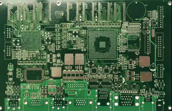
There are many classification methods for PCBs, which can be classified as follows according to the number of conductive layers, bending toughness, assembly method, substrate, special functions, wire forming process, presence or absence of core plate, and surface treatment method.
(1) According to the number of conductive layers, it can be divided into single panel, double-sided panel and multilayer panel. multilayer boards can be divided into ordinary Multilayer boards and laminated multilayer boards according to the number of laminations (the core is the position of the hole, and the position of the hole determines the number of laminations).
In ordinary multilayer boards, more than 12 layers are generally referred to as high layer count boards, and those with more than 16 layers, aperture greater than 0.3mm, thickness diameter ratio greater than or equal to 8 are referred to as backplanes.
Build up multi layer PCB, also known as layer adding multilayer board (the products represented by the micro viamulti layer and multilayer multilayer board, which are often referred to in the industry, are basically the same). The typical product of built-up multilayer board is HDI PCB, which is calLED High Density Interconnection in full. Generally, the minimum line width/spacing is 0.075/0.075mm or less, the minimum hole diameter is 0.15 mm or less, and there are blind The conditions such as buried hole are called HDI.
HDI includes Level 1, Level 2, and High Level (Level 3 and above, currently, Level 3 and Level 4 are more commonly used in terminal products, and Level 4 and above are basically converted to Any layer), Any layer (any level, or any layer, also known as ELIC (Every Layer Interconnect) by some companies), and SLP (Substrate Like PCB, SIMilar carrier board). Currently, 10 and 12 layers of Any Layer and SLP are more commonly used in high-end terminal products.
(2) According to bending toughness, it can be divided into: Rigid printed circuit, Flexible Printed Circuit (FPC), rigid flexible printed circuit (HDI), and rigid flexible printed circuit (HDI).
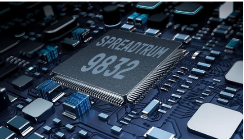
(3) According to the assembly mode, it can be divided into: through hole plug-in PCB, surface mount PCB, and chip level packaging PCB. PCB for chip level packaging, which is often called Substrate or IC Substrate (also called IC Carrier) in the industry, is translated as (chip level) packaging carrier. It is not recommended that the industry use the confusing and inaccurate name of packaging substrate; In addition, the view that Substrate does not belong to PCB is also inaccurate).
Substrate generally includes two types: FCBGA (Flip Chip Ball GridArray) in unit base and BGA (Ball Grid Array) in strip base.
FCBGA has a single type, usually 4-16 layers (the manufacturing difficulty is the most difficult among all PCB products). BGA has a wide variety, including BOC (Board on Chip), PBGA (Plastic Ball Grid Array), CSP (Chip scale Packaging), SiP (System in package), FCCSP (Flip Chip Ball Grid Array), etc. The common layers are 1-10.
(4) According to the base material, it can be divided into phenolic paper base, epoxy glass fiber cloth, PI (polyimide), BT (biSMAleimide triazine resin), PTFE (polytetrafluoroethylene), ceramic base, metal base, etc.
(5) According to special functions, it can be divided into: embedded component board (embedded passive components internally or passive components with special materials on the surface, and embedded active components internally), carbon fiber substrate, photoelectric printed board, etc.
(6) According to the wire forming process, it can be divided into: Subtractive (or Tenting, where the core is to form a line after thickening on conventional copper), MSAP/MSAP+(Modified SEMI Additive Process, where the core is to thicken the line while forming on thin copper), SAP (Semi Additive Process, where the core is to thicken the line while plating ultra-thin copper on insulating substrate), etc.
(7) It can be divided into Cored and Coreless according to whether there is core. Coreless can be divided into ordinary Coreless and ETS (Embedded Trace Substrate, or EPP, Embedded Pattern Process, embedded circuit board or flush board).
(8) It can be divided into tin plating, gold plating (nickel gold, nickel palladium, hard gold and soft gold), silver plating, OSP, SOP (Solder On Pad, also known as Bump), etc. according to the surface treatment method. In fact, SOP is a proprietary and main surface treatment method of the aforementioned FCCSP products (the other is OSP, which has low cost but few applications). The general FCCSP packaging is more complex PoP packaging (Packaging on Packaging, which usually packages two different types of chips in one module).
However, in practice, we often see a mixed classification method: single panel, double-sided board, multilayer board, HDI board, packaging carrier board, flexible board, rigid flex joint board, and special board, which is mainly based on the output value of each subdivided product in the entire PCB industry.
Look at the analysis of PCB welding process
11-07,2022


抖音二維碼

Q Q二維碼

微信二維碼
點(diǎn)擊
然后
聯(lián)系
然后
聯(lián)系
電話熱線
13410863085Q Q

微信

- 郵箱